LC863096 Ver la hoja de datos (PDF) - SANYO -> Panasonic
Número de pieza
componentes Descripción
Lista de partido
LC863096 Datasheet PDF : 20 Pages
| |||
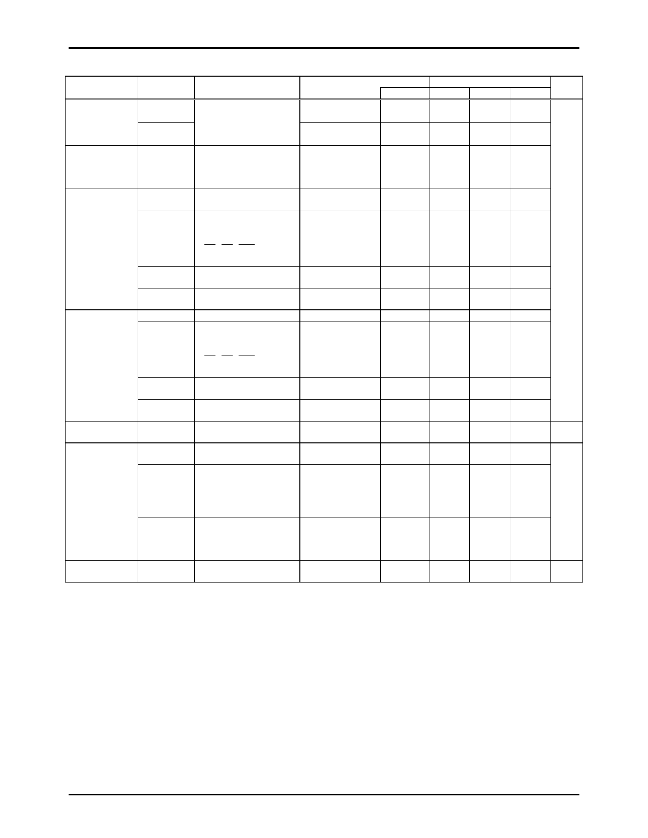
LC863232/28/24/20/16A
2. Recommended Operating Range at Ta=-10°C to +70°C, VSS=0V
Parameter
Symbol
Pins
Operating
supply voltage
range
VDD(1)
VDD(2)
VDD
Hold voltage
VHD
VDD
High level input
voltage
VIH(1)
VIH(2)
VIH(3)
VIH(4)
Low level input VIL(1)
voltage
VIL(2)
CVIN
Operation
cycle time
VIL(3)
VIL(4)
VCVIN
tCYC(1)
tCYC(2)
Port 0 (Schumitt)
•Ports 1,6 (Schumitt)
•Port 7 (Schumitt)
port input/interrupt
• HS , VS , RES
(Schumitt)
Port 70
Watchdog timer input
•Port 8
port input
Port 0 (Schumitt)
•Ports 1,6 (Schumitt)
•Port 7 (Schumitt)
port input/interrupt
• HS , VS , RES
(Schumitt)
Port 70
Watchdog timer input
Port 8
port input
CVIN
tCYC(3)
Oscillation
FmRC
frequency range
Conditions
VDD[V]
Ratings
min.
typ.
max.
unit
0.844µs ≤ tCYC ≤
0.852µs
4.5
5.5
V
4µs ≤ tCYC ≤
400µs
4.5
5.5
RAMs and the
2.0
5.5
registers data are
kept in HOLD
mode.
Output disable
4.5 - 5.5 0.6VDD
VDD
Output disable
4.5 - 5.5 0.75VDD
VDD
Output disable
Output disable
Output disable
Output disable
4.5 - 5.5 VDD-0.5
4.5 - 5.5 0.7VDD
4.5 - 5.5 VSS
4.5 - 5.5 VSS
VDD
VDD
0.2VDD
0.25VDD
Output disable
4.5 - 5.5
Output disable
4.5 - 5.5
5.0
•All functions
operating
•AD converter
operating
•OSD and Data
slicer are not
operating
•OSD, AD
converter and
Data slicer are not
operating
Internal RC
oscillation
4.5 - 5.5
4.5 - 5.5
4.5 - 5.5
4.5 - 5.5
VSS
VSS
1Vp-p
-3dB
0.844
0.844
0.844
0.4
0.6VDD
0.3VDD
1Vp-p 1Vp-p Vp-p
+3dB
*
0.848 0.852 µs
30
400
0.8
3.0 MHz
* Vp-p : Peak-to-peak voltage
No.6693-10/20
Share Link: 