MB88154-102 Ver la hoja de datos (PDF) - Fujitsu
Número de pieza
componentes Descripción
Lista de partido
MB88154-102 Datasheet PDF : 18 Pages
| |||
MB88154
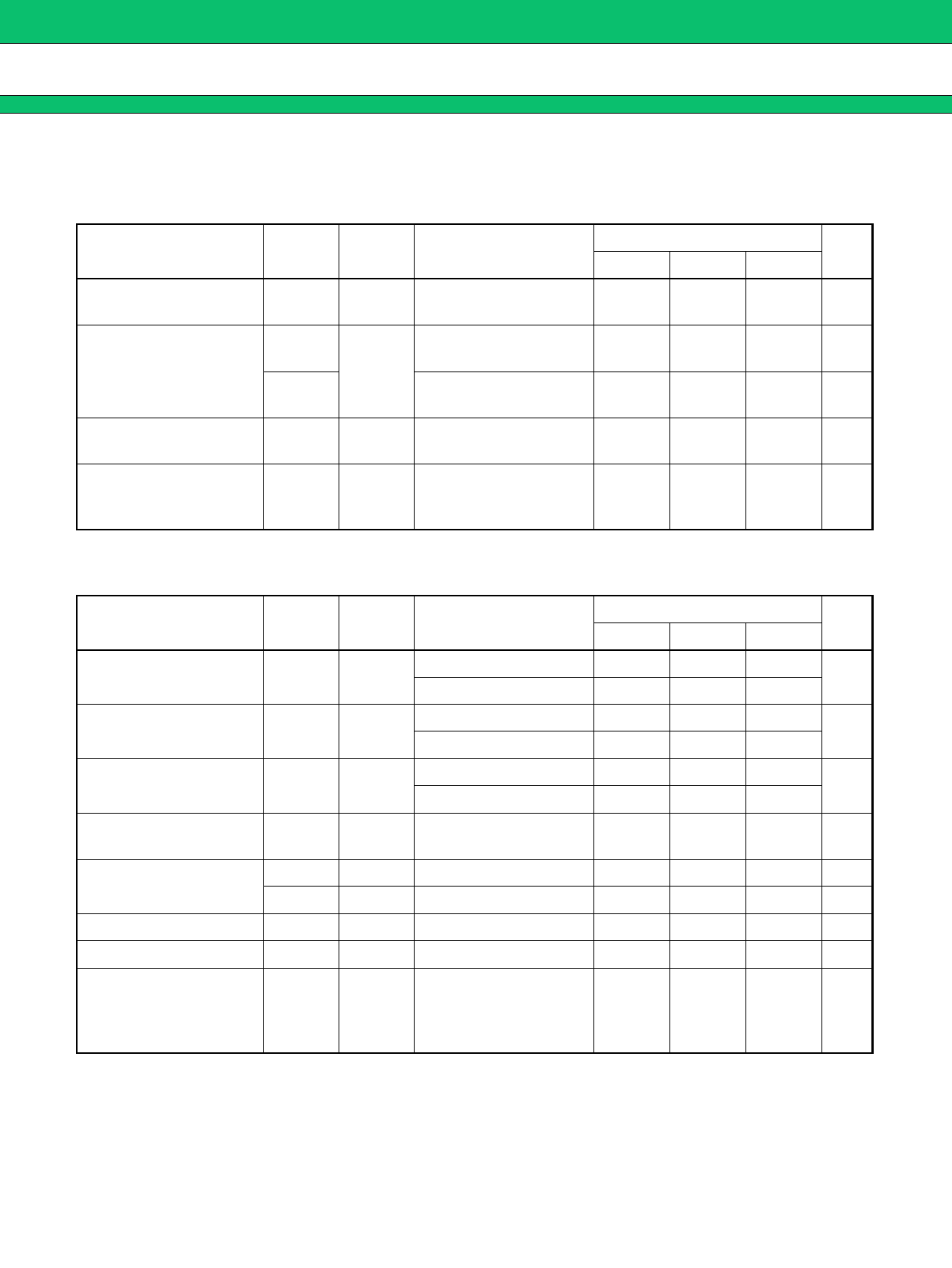
■ ELECTRICAL CHARACTERISTICS
• DC Characteristics
(Ta = −40 °C to + 85 °C, VDD = 3.3 V ± 0.3 V, VSS = 0.0 V)
Parameter
Symbol Pin
Conditions
Value
Unit
Min
Typ
Max
Power supply current
ICC
VDD
no load capacitance at
24 MHz output
⎯
5.0
7.0 mA
Output voltage
VOH
CKOUT,
REFOUT
VOL
“H” level output
IOH = − 3 mA
“L” level output
IOL = 3 mA
VDD − 0.5
⎯
VSS
⎯
VDD
V
0.4
V
Output impedance
ZO
CKOUT,
REFOUT
16.6 MHz to 67 MHz
⎯
70
⎯
Ω
Input capacitance
XIN,
Ta = + 25 °C,
CIN
SEL0,
VDD = VI = 0.0 V,
⎯
⎯
16
pF
SEL1
f = 1 MHz
• AC Characteristics
Parameter
Oscillation frequency
Input frequency
Output frequency
Output slew rate
Output clock duty cycle
Modulation frequency
Lock-Up time
Cycle-cycle jitter
(Ta = −40 °C to + 85 °C, VDD = 3.3 V ± 0.3 V, VSS = 0.0 V)
Symbol Pin
Conditions
Value
Unit
Min
Typ
Max
fx
XIN, Fundamental oscillation 16.6
XOUT 3rd over-tone oscillation 40
⎯
⎯
40
MHz
48
MB88154-103/113
16.6
⎯
fin
XIN
MB88154-102/112
33
⎯
40
MHz
67
fOUT
CKOUT,
REFOUT
MB88154-103/113
MB88154-102/112
16.6
33
⎯
⎯
40
MHz
67
SR
CKOUT,
0.4 V to 2.4 V
REFOUT load capacitance 15 pF
0.3
⎯
2.0 V/ns
tDCC CKOUT
1.5 V
40
⎯
60
%
tDCR REFOUT
1.5 V
tDCI − 10*
⎯
tDCI + 10* %
fMOD CKOUT
⎯
⎯
12.5
⎯
kHz
tLK
CKOUT
⎯
⎯
2
5
ms
No load capacitance,
tJC
CKOUT
Ta = +25 °C,
VDD = 3.3 V,
⎯
Standard deviation σ
⎯
100
ps
* : Duty of the REFOUT output is guaranteed only for the following A and B because it depends on tDCI of input
clock duty.
A. Resonator : When resonator is connected with XIN and XOUT and oscillates normally.
B. External clock input : The input level is Full - swing (VSS − VDD).
9
Share Link: 