SL34118 Ver la hoja de datos (PDF) - System Logic Semiconductor
Número de pieza
componentes Descripción
Lista de partido
SL34118 Datasheet PDF : 12 Pages
| |||
SL34118
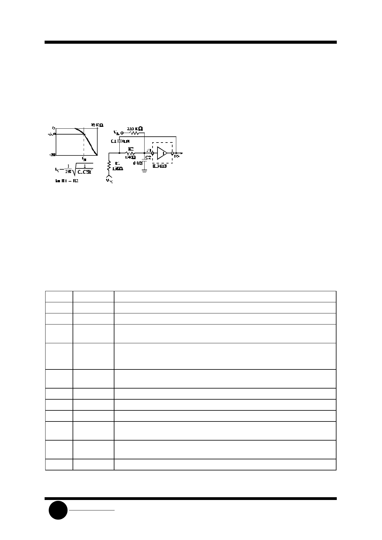
As a low pass filter (Figure 7), it can be used to
roll off the high and frequencies in the receive circuit,
which aids protecting against acoustic feedback
problems. With an appropriate choice of an input
coupling capacitor to the low pass filter, a band pass
filter is formed.
Figure 7. Low Pass Filter
POWER SUPPLY, VB, AND CHIP
DISABLE
The power supply voltage at VCC (Pin 4) is to be
between 3.5 and 6.5 volts for normal operation, with
reduced operation possible down to 2.8 volts.
The output voltage at VB (Pin 15) is ≈(VCC - 0.7)/2, and
provides the ac ground for the system. The output
impedance at VB is ≈400 Ω, and in conjunction with
the external capacitor at VB, forms a low pass filter for
power supply rejection.
Since VB biases the microphone and hybrid
amplifiers, the amount of supply rejection at their
outputs is directly related to the rejection at VB, as
well as their respective gains.
The Chip Disable (Pin 3) permits powering down
the IC to conserve power and/or for muting purposes.
With CD≤0.8 volts, normal operation is in effect. With
CD≥2.0 volts and ≤VCC, the IC is powered down. In
the powered down mode, the microphone and the
hybrid amplifiers are disabled, and their outputs go to
a high impedance state. Additionally, the bias is
removed from the filter (Pins 1, 2), the attenuators
(Pins 8, 9, 21, 22), or from Pins 13, 14, and 15 (the
attenuators are disabled, however, and will not pass a
signal). The input impedance at CD is typically 90 kΩ,
has a threshold of ≈1.5 volts, and the voltage at this
pin must be kept within the range of ground and VCC.
If CD is not used, the pin should be grounded.
PIN DESCRIPTION
Pin No Designation
Description
1
FO
Filter output. Output impedance is less than 50Ω.
2
FI
Filter input. Input impedance is greater than 1.0 MΩ.
3
CD
Chip Disable. A logic low (<0.8 V) sets normal operation. A logic high (>2.0 V)
disables the IC to conserve power. Input impedance is nominally 90 KΩ.
4
VCC
A supply voltage of +2.8 to +6.5 Volts is required, at ≈5.0 mA. As VCC falls from 3.5
to 2.8 Volts, an AGC circuit reduces the receive attenuator gain by ≈25 dB (when in
the receive mode).
5
HTO+ Output of the second hybrid amplifier. The gain is internally set at -1.0 to provide a
differential output, in conjunction with HTO-, to the hybrid transformer.
6
HTO-
Output of the first hybrid amplifier. The gain of the amp is set by external resistors.
7
HTI
Input and summing node for the first hybrid amplifier. DC level is ≈VB.
8
TXO
Output of the transmit attenuator. DC level is approximately VB.
9
TXI
Input to the transmit attenuator. Max. signal level is 350 mVrms. Input impedance is
≈10 KΩ.
10
MCO
Output of the microphone amplifier. The gain of the amplifier is set by external
resistors.
11
MCI
Input and summing node of the microphone amplifier. DC level is ≈VB.
PIN DESCRIPTION
(continued)
SLS
System Logic
Semiconductor
Share Link: 