NTE931 Ver la hoja de datos (PDF) - NTE Electronics
Número de pieza
componentes Descripción
Lista de partido
NTE931 Datasheet PDF : 2 Pages
| |||
Electrical Characteristics: (TJ = 0° to +125°C, Note 2 unless otherwise specified)
Parameter
Output Voltage
Line Regulation
Load Regulation
Quiescent Current
Output Noise Voltage
Short Circuit Current Limit
Long Term Stability
Symbol
Test Conditions
VO
Regline
Regload
TJ = +25°C, VIN = 7.5V, IO = 0A
VIN = 7.5V to 15V, IO = 0A to 3A, P ≤ 30W
TJ = +25°C, VIN = 7.5V to 15V, Note 3
TJ = +25°C, VIN = 7.5V, IO = 0A to 3A, Note 3
IB VIN = 7.5V to 15V, IO = 0A to 3A
Vn TJ = +25°C, f = 10Hz to 100kHz
TJ = +25°C, VIN = 15V
TJ = +25°C, VIN = 7.5V
Min Typ Max Unit
4.8 5.0 5.2 V
4.75 5.00 5.25 V
–
5 25 mV
– 25 100 mV
– 12 20 mA
–
40
– µVrms
– 3.0 4.5 A
– 4.0 5.0 A
–
– 35 mW
Note 2. Although power dissipation is internally limited, specifiecations apply only for P ≤ 30W.
Note 3. Load and line regulation are specified at constant junction temperature. Pulse testing is
required with a pulse width of ≤ 1ms and a duty cycle of ≤ 5%.
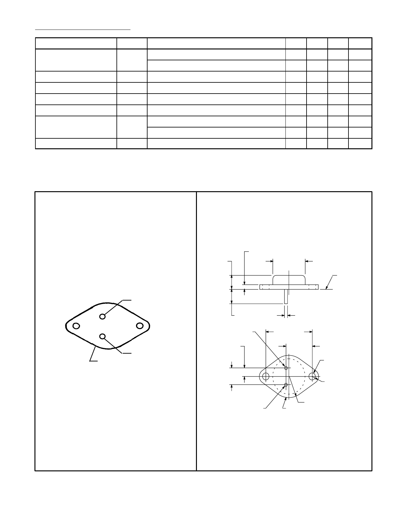
Pin Connection Diagram
Output
2
1
Input
Case/GND
.350 (8.89)
.135 (3.45) Max
.875 (22.2)
Dia Max
Seating
Plane
.312 (7.93) Min
.040 (1.02)
VOUT
.215 (5.45)
.430
(10.92)
1.187 (30.16)
.665
(16.9)
.156 (3.96) Dia
(2 Holes)
.188 (4.8) R Max
.525 (13.35) R Max
VIN
GND/Case
Share Link: 