CMX631A Ver la hoja de datos (PDF) - CML Microcircuits
Número de pieza
componentes Descripción
Lista de partido
CMX631A Datasheet PDF : 16 Pages
| |||
Low Voltage SPM Detector
3 External Components
CMX631A
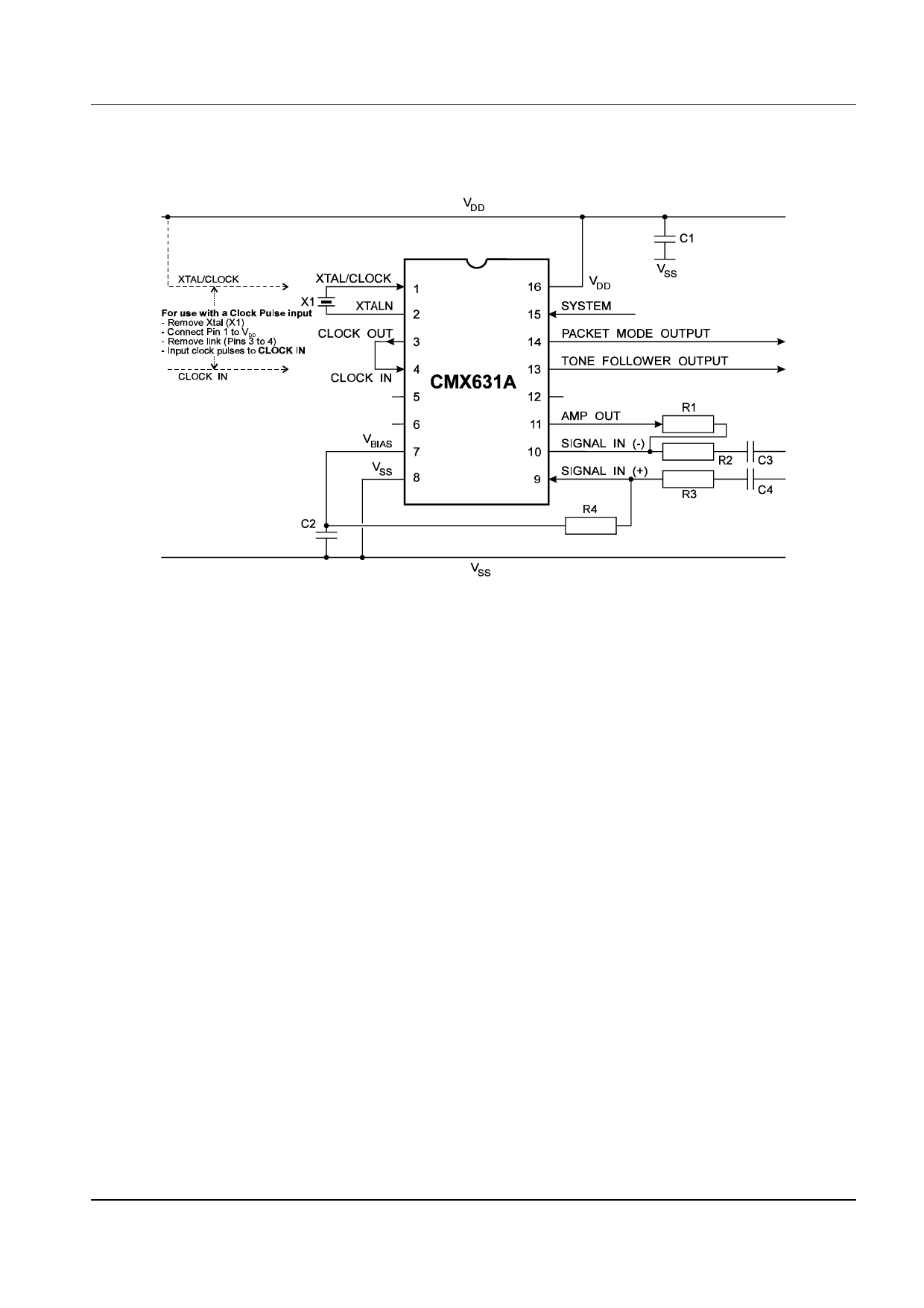
Figure 2: Recommended External Components
R1 Note 1
R2 Note 1
R3 Note 1
R4 Note 1
RFEEDBACK
RIN(-)
RIN(+)
RBIAS
C1
1.0µF
C2
1.0µF
C3
CIN(-)
C4
CIN(+)
X1 Note 2, 3, 4 3.579545MHz
Table 2: Recommended External Components
±20%
±20%
Recommended External Component Notes:
1. When calculating input gain components, for correct operation R1 and R4 should always be ≥ 33kΩ.
2. For best results, a crystal oscillator design should drive the clock inverter input with signal levels of at
least 40% of VDD, peak to peak. Tuning fork crystals generally cannot meet this requirement. To obtain
crystal oscillator design assistance, consult your crystal manufacturer.
3. The on-chip crystal circuitry includes a feedback resistor (nominally 2MΩ) between pins 1 and 2 and
load capacitors on pins 1 and 2 (nominally 10pF each, excluding package and board parasitics).
4. When using an external clock input, X1 should be removed, Pin 1 (Xtal/Clock) should be tied to VDD,
the Clock In and Clock Out jumper should be removed, and the external clock signal applied to Clock In.
© 1998 Consumer Microcircuits Limited
5
D/631A/1
Share Link: 