LC86E4564 Ver la hoja de datos (PDF) - SANYO -> Panasonic
Número de pieza
componentes Descripción
Lista de partido
LC86E4564 Datasheet PDF : 19 Pages
| |||
LC86E4564
Specifications
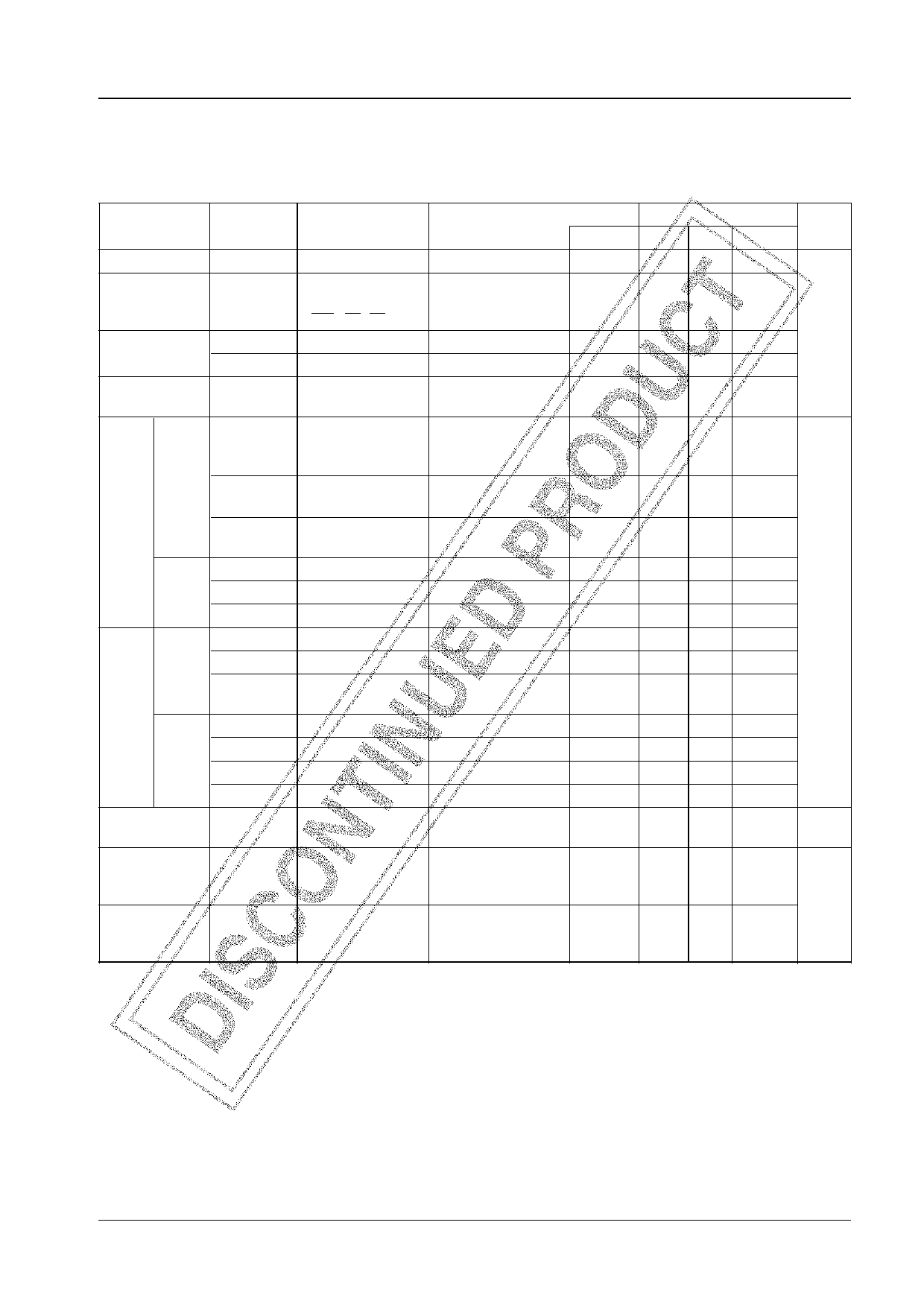
1. Absolute Maximum Ratings at Ta = 25°C, VSS = 0 V
Parameter
Supply voltage
Input voltage
Output voltage
Input/output
voltage
High-
level
output
current
Peak
output
current
Total
output
current
Low-
level
output
current
Peak
output
current
Total
output
current
Maximum power
dissipation
Operating
temperature
range
Storage
temperature
range
Symbol
Pins
VDDmax
VI(1)
VO(1)
VO(2)
VIO(1)
IOPH(1)
DVDD, AVDD
• P71, 72, 73
• Port 9
• RES, HS, VS
R, G, B, BL, FILT
PWM0 to PWM9
Ports 0, 1, P70
DA0, 1
Ports 0, 1
IOPH(2)
IOPH(3)
Ports 0, 1
DA0, 1
R, G, B, BL
∑IOAH(1)
∑IOAH(2)
∑IOAH(3)
IOPL(1)
IOPL(2)
IOPL(3)
∑IOAL(1)
∑IOAL(2)
∑IOAL(3)
∑IOAL(4)
Pd max
Port 1
Port 0
R, G, B, BL
Ports 0, 1 DA0, 1
P70
• R, G, B, BL
• PWM0 to PWM9
Port 0
Port 1, P70
R, G, B, BL
PWM0 to PWM9
DIC52S
Conditions
DVDD = AVDD
VDD [V]
• Pull-up MOS transistor
output
• At each pin
• CMOS output
• At each pin
• CMOS output
• At each pin
The total of all pins
The total of all pins
The total of all pins
At each pin
At each pin
At each pin
The total of all pins
The total of all pins
The total of all pins
The total of all pins
Ta = +10 to +40°C
Ratings
Unit
min typ
max
–0.3
+7.0 V
–0.3
VDD+0.3
–0.3
–0.3
–0.3
–2
VDD+0.3
+15
VDD+0.3
mA
–4
–5
–10
–10
–15
20
30
5
40
40
15
30
600 mW
Topr
10
+40 °C
Tstg
–55
+150
* DVSS and AVSS must be supplied the same voltage, VSS.
DVDD and AVDD must be supplied the same voltage, VDD.
VSS = DVSS = AVSS
VDD = DVDD = AVDD
No. 5584-9/19
Share Link: 