LC89962 Ver la hoja de datos (PDF) - SANYO -> Panasonic
Número de pieza
componentes Descripción
Lista de partido
LC89962 Datasheet PDF : 6 Pages
| |||
LC89962, LC89962M
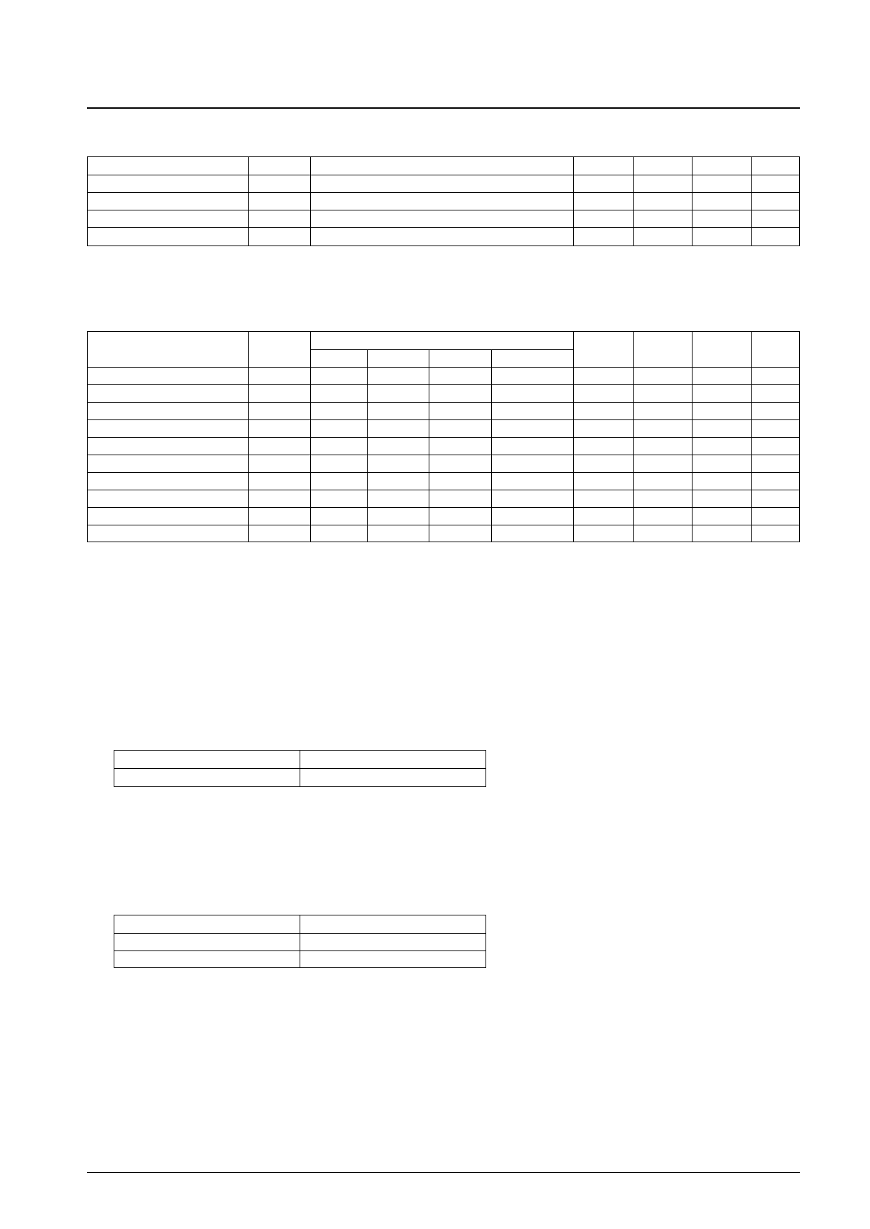
Allowable Operating Ranges at Ta = 25°C
Parameter
Symbol
Conditions
Supply voltage
Clock input amplitude
Clock frequency
Signal input amplitude
VDD
VCLK
FCLK
VIN
Sine wave
(*1)
Note 1. The input signal must be input with low impedance for correct operation of sync-tip clamping.
min
typ
4.75
5.0
200
300
3.579545
500
max
5.25
500
572
Unit
V
mVp–p
MHz
mVp–p
Electrical Characteristics at Ta = 25°C, VDD = 5.0 V, CLK = 3.579545 MHz; 300 mV p-p
Parameter
Supply current
Voltage gain
Frequency characteristics
Differential gain
Differential phase
Linearity
Clock leakage
Noise
Output impedance
Delay time
Symbol
IDD
GV
Gf
DG
DP
LS
Lck
NO
ZO
TD
SW1
a
a
b
a
a
a
a
a
a
a
Switch states
SW2
min
SW3 Test conditions
a
a
*1
5
b
a
*2
–2
b
a
*3
–2
a
a
*4
0
a
a
*4
0
a
a
*5
37
b
a
*6
b
a
*7
b
a↔b
*8
220
b
a
*9
typ
15
0
–1
5
5
40
5
1
370
63.33
max
Unit
25
mA
+2
dB
0
dB
%
deg
43
%
50
mVrms
2
mVrms
520
Ω
µs
Test Conditions
1. The supply current with no input signal
2. The following formula is used to calculate the voltage gain (GV).
GV
=
20log
—V—OU—T —[m—Vp—-p—]
500 [mVp-p]
[dB]
Output signal symbol
VOUT
Input signal
Sine wave: 200 kHz, 500 mV p-p
3. The following formula is used to calculate the frequency characteristics (Gf).
V2 [mVp-p]
Gf
=
20log
——————
V1 [mVp-p]
[dB]
Output signal symbol
V1
V2
Input signal
Sine wave: 200 kHz, 200 mV p-p
Sine wave: 3.58 MHz, 200 mV p-p
During this test, adjust Vbias so that the input signal DC level is 250 mV higher than the clamp level.
No. 5420-2/6
Share Link: 