MC74VHCT540ADTR2 Ver la hoja de datos (PDF) - ON Semiconductor
Número de pieza
componentes Descripción
Lista de partido
MC74VHCT540ADTR2 Datasheet PDF : 8 Pages
| |||
MC74VHCT540A
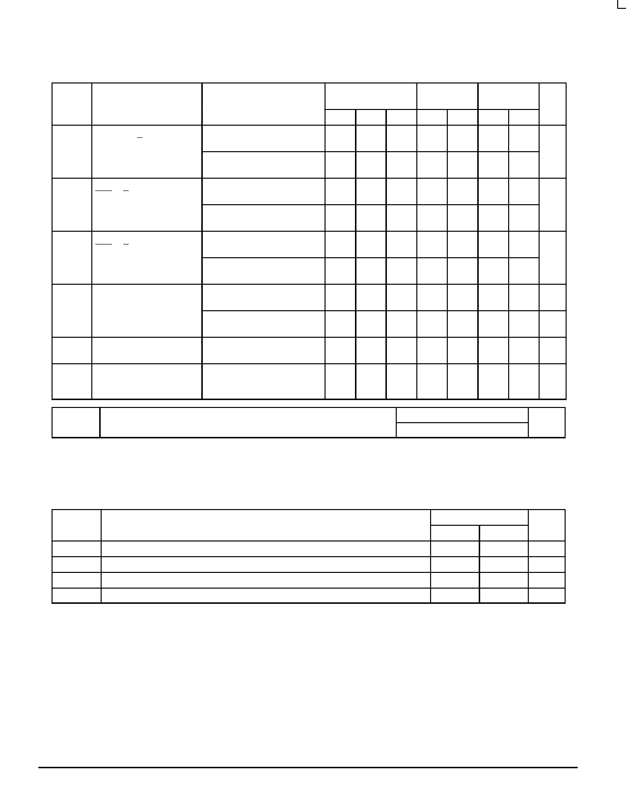
ÎÎÎÎÎÎÎÎÎÎÎÎÎÎÎÎÎÎÎÎÎÎÎÎÎÎÎÎÎÎÎÎÎ AC ELECTRICAL CHARACTERISTICS (Input tr = tf = 3.0ns)
ÎÎÎÎÎÎÎÎÎÎÎÎÎÎÎÎÎÎÎÎÎÎÎÎÎÎÎÎÎÎÎÎÎÎÎÎÎÎÎÎÎÎÎÎÎÎÎÎÎÎÎÎÎÎÎÎÎÎÎÎÎÎÎÎÎÎÎÎÎÎÎÎÎÎÎÎÎÎÎÎÎÎÎÎÎÎÎÎÎÎÎÎÎÎÎÎÎÎÎ Symbol
Parameter
Test Conditions
ÎÎÎÎÎÎÎÎÎÎÎÎÎÎÎÎÎÎÎÎÎÎÎÎÎÎÎÎÎÎÎÎÎ tPLH,
ÎÎÎÎÎÎÎÎÎÎÎÎÎÎÎÎÎÎÎÎÎÎÎÎÎÎÎÎÎÎÎÎÎ tPHL
Maximum Propagation
Delay, A to Y
(Figures 1 and 3)
ÎÎÎÎÎÎÎÎÎÎÎÎÎÎÎÎÎÎÎÎÎÎÎÎÎÎÎÎÎÎÎÎÎÎÎÎÎÎÎÎÎÎÎÎÎÎÎÎÎÎÎÎÎÎÎÎÎÎÎÎÎÎÎÎÎÎ tPZL,
ÎÎÎÎÎÎÎÎÎÎÎÎÎÎÎÎÎÎÎÎÎÎÎÎÎÎÎÎÎÎÎÎÎ tPZH
Output Enable TIme,
OEn to Y
(Figures 2 and 4)
ÎÎÎÎÎÎÎÎÎÎÎÎÎÎÎÎÎÎÎÎÎÎÎÎÎÎÎÎÎÎÎÎÎÎÎÎÎÎÎÎÎÎÎÎÎÎÎÎÎÎÎÎÎÎÎÎÎÎÎÎÎÎÎÎÎÎ tPLZ,
ÎÎÎÎÎÎÎÎÎÎÎÎÎÎÎÎÎÎÎÎÎÎÎÎÎÎÎÎÎÎÎÎÎÎÎÎÎÎÎÎÎÎÎÎÎÎÎÎÎÎÎÎÎÎÎÎÎÎÎÎÎÎÎÎÎÎ tPHZ
Output Disable Time,
OEn to Y
(Figures 2 and 4)
ÎÎÎÎÎÎÎÎÎÎÎÎÎÎÎÎÎÎÎÎÎÎÎÎÎÎÎÎÎÎÎÎÎÎÎÎÎÎÎÎÎÎÎÎÎÎÎÎÎÎÎÎÎÎÎÎÎÎÎÎÎÎÎÎÎÎ tOSLH, OutputtoOutputSkew
ÎÎÎÎÎÎÎÎÎÎÎÎÎÎÎÎÎÎÎÎÎÎÎÎÎÎÎÎÎÎÎÎÎÎÎÎÎÎÎÎÎÎÎÎÎÎÎÎÎÎÎÎÎÎÎÎÎÎÎÎÎÎÎÎÎÎ tOSHL
VCC = 3.3 ± 0.3V
VCC = 5.0 ± 0.5V
VCC = 3.3 ± 0.3V
RL = 1kΩ
VCC = 5.0 ± 0.5V
RL = 1kΩ
VCC = 3.3 ± 0.3V
RL = 1kΩ
VCC = 5.0 ± 0.5V
RL = 1kΩ
VCC = 3.3 ± 0.3V
(Note 1.)
VCC = 5.0 ± 0.5V
(Note 1.)
CL = 15pF
CL = 50pF
CL = 15pF
CL = 50pF
CL = 15pF
CL = 50pF
CL = 15pF
CL = 50pF
CL = 50pF
CL = 50pF
CL = 50pF
CL = 50pF
ÎÎÎÎÎÎÎÎÎÎÎÎÎÎÎÎÎÎÎÎÎÎÎÎÎÎÎÎÎÎÎÎÎ Cin MaximumInput
ÎÎÎÎÎÎÎÎÎÎÎÎÎÎÎÎÎÎÎÎÎÎÎÎÎÎÎÎÎÎÎÎÎ Capacitance
ÎÎÎÎÎÎÎÎÎÎÎÎÎÎÎÎÎÎÎÎÎÎÎÎÎÎÎÎÎÎÎÎÎÎÎÎÎÎÎÎÎÎÎÎÎÎÎÎÎÎÎÎÎÎÎÎÎÎÎÎÎÎÎÎÎÎÎÎÎÎÎÎÎÎÎÎÎÎÎÎÎÎÎÎÎÎÎÎÎÎÎÎÎÎÎÎÎÎÎ Cout
Maximum Three–State
Output Capacitance (Output
in High Impedance State)
TA = 25°C
Min Typ Max
4.8 7.0
7.3 10.5
3.7 5.0
5.2 7.0
6.8 10.5
9.3 14.0
4.7 7.2
6.2 9.2
11.2 15.4
6.0 8.8
1.5
1.0
4
10
6
TA = – 40 to
85°C
Min Max
1.0 8.5
1.0 12.0
1.0 6.0
1.0 8.0
1.0 12.5
1.0 16.0
1.0 8.5
1.0 10.5
1.0 17.5
1.0 10.0
1.5
1.0
10
TA ≤ 125°C
Min Max Unit
10.5 ns
14.0
8.0
10.0
15.0 ns
19.0
10.5
13.0
20.0 ns
11.5
2.0 ns
1.5 ns
10 pF
pF
Typical @ 25°C, VCC = 5.0V
CPD Power Dissipation Capacitance (Note 2.)
17
pF
1. Parameter guaranteed by design. tOSLH = |tPLHm – tPLHn|, tOSHL = |tPHLm – tPHLn|.
2. CPD is defined as the value of the internal equivalent capacitance which is calculated from the operating current consumption without load.
Average operating current can be obtained by the equation: ICC(OPR) = CPD VCC fin + ICC / 8 (per bit). CPD is used to determine the no–load
dynamic power consumption; PD = CPD VCC2 fin + ICC VCC.
NOISE CHARACTERISTICS (Input tr = tf = 3.0ns, CL = 50pF, VCC = 5.0V)
Symbol
VOLP
VOLV
VIHD
VILD
Parameter
Quiet Output Maximum Dynamic VOL
Quiet Output Minimum Dynamic VOL
Minimum High Level Dynamic Input Voltage
Maximum Low Level Dynamic Input Voltage
TA = 25°C
Typ
Max
Unit
0.9
1.2
V
– 0.9
– 1.2
V
3.5
V
1.5
V
VHC Data – Advanced CMOS Logic
3
DL203 — Rev 2
MOTOROLA
Share Link: 