IRF7204 Ver la hoja de datos (PDF) - International Rectifier
Número de pieza
componentes Descripción
Lista de partido
IRF7204 Datasheet PDF : 9 Pages
| |||
IRF7204
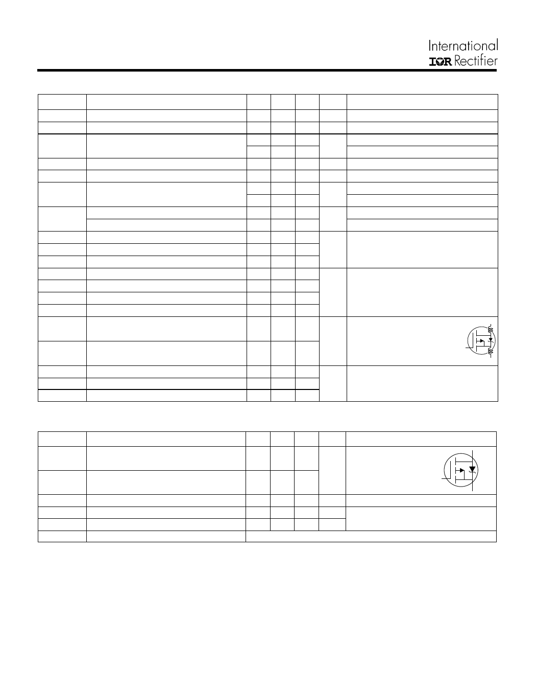
Electrical Characteristics @ TJ = 25°C (unless otherwise specified)
Parameter
V(BR)DSS Drain-to-Source Breakdown Voltage
∆V(BR)DSS/∆TJ Breakdown Voltage Temp. Coefficient
RDS(ON)
Static Drain-to-Source On-Resistance
VGS(th)
gfs
Gate Threshold Voltage
Forward Transconductance
IDSS
Drain-to-Source Leakage Current
IGSS
Qg
Qgs
Qgd
td(on)
tr
td(off)
tf
Gate-to-Source Forward Leakage
Gate-to-Source Reverse Leakage
Total Gate Charge
Gate-to-Source Charge
Gate-to-Drain ("Miller") Charge
Turn-On Delay Time
Rise Time
Turn-Off Delay Time
Fall Time
LD
Internal Drain Inductance
LS
Internal Source Inductance
Ciss
Input Capacitance
Coss
Output Capacitance
Crss
Reverse Transfer Capacitance
Min. Typ. Max. Units
Conditions
-20 ––– –––
––– -0.022 –––
––– ––– 0.060
––– ––– 0.10
V
V/°C
Ω
VGS = 0V, ID = -250µA
Reference to 25°C, ID = -1mA
VGS = -10V, ID = -5.3A
VGS = -4.5V, ID = -2.0A
-1.0 ––– -2.5 V
––– 7.9 ––– S
––– ––– -25
µA
––– ––– -250
––– ––– -100 nA
––– ––– 100
VDS = VGS, ID = -250µA
VDS = -15V, ID = -5.3A
VDS = -16V, VGS = 0V
VDS = -16V, VGS = 0V, TJ = 125 °C
VGS = -12V
VGS = 12V
––– 25 –––
––– 5.0 –––
––– 8.0 –––
––– 14 30
ID = -5.3A
nC VDS = -10V
VGS = -10V
VDD = -10V
––– 26 60 ns ID = -1.0A
––– 100 150
RG = 6.0Ω
––– 68 100
RD = 10Ω
D
––– 2.5 –––
nH Between lead,6mm(0.25in.)
from package and center G
––– 4.0 –––
of die contact
S
––– 860 –––
––– 750 –––
––– 230 –––
VGS = 0V
pF VDS = -10V
ƒ = 1.0MHz
Source-Drain Ratings and Characteristics
Parameter
IS
Continuous Source Current
(Body Diode)
ISM
Pulsed Source Current
(Body Diode)
V SD
Diode Forward Voltage
trr
Reverse Recovery Time
Qrr
Reverse RecoveryCharge
ton
Forward Turn-On Time
Min. Typ. Max. Units
Conditions
––– ––– -2.5
––– ––– -15
––– ––– -1.2
––– 85 100
––– 77 120
MOSFET symbol
D
showing the
A
integral reverse
G
p-n junction diode.
S
V TJ = 25°C, IS = -1.25A, VGS = 0V
ns TJ = 25°C, IF = -2.4A
nC di/dt = 100A/µs
Intrinsic turn-on time is negligible (turn-on is dominated by LS+LD)
Notes:
Repetitive rating; pulse width limited by
max. junction temperature.
Pulse width ≤ 300µs; duty cycle ≤ 2%.
ISD ≤ -5.3A, di/dt ≤ 90A/µs, VDD ≤ V(BR)DSS,
TJ ≤ 150°C
Surface mounted on FR-4 board, t ≤ 10sec.
Share Link: 