RF9986PCBA Ver la hoja de datos (PDF) - RF Micro Devices
Número de pieza
componentes Descripción
Lista de partido
RF9986PCBA Datasheet PDF : 8 Pages
| |||
RF9986
Pin
20
21
22
23
24
Function
LNA OUT
GND8
VCC4
GND9
NC
Description
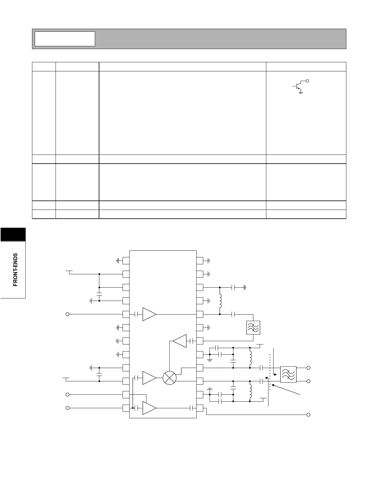
Interface Schematic
LNA output pin. This is an open-collector output. This pin is typically
connected to pin 22 through a bias/matching inductor. This inductor, in
LNA
OUT
conjunction with a series blocking/matching capacitor, forms a match-
ing network to the 50Ω image filter and provides bias (see Application
Schematic). The LNA’s IP3 may be increased 10dB by connecting pin
20 to VCC through the inductor. The LNA’s current then increases by
10mA. Other in-between IP3 vs. ICC trade-offs may be made by con-
necting resistance values between VCC and the matching inductor. The
two reference points for consideration are with 150Ω used, which is
what connection to pin 22 achieves, the Input IP3 is +5.5dBm and the
LNA ICC is 5mA. Using no resistance, the Input IP3 is +15.5 dBm and
the LNA ICC is 15 mA. Desired operating points in between these val-
ues may be interpolated, roughly.
Same as pin 17.
Output supply voltage for the LNA output (pin 20). This pin is typically
connected to pin 20 through a bias/matching inductor (see application
schematic). External RF bypassing is required. The trace length
between the pin and the bypass capacitor should be minimized. The
ground side of the bypass capacitor should connect immediately to
ground plane.
Same as pin 17.
See pin 2.
No connection. This pin may be grounded (recommended) or left open.
8
Application Schematic
1
VCC
2
3
22 pF
4
24
23
22 pF
22
21
2.7 nH
RF IN
VCC
LO BUFF EN
(On: ≥3.1 V;
Off: ≤0.5 V)
LO IN
5
6
7
8
9
22 pF
10
11
12
20
1.8 pF
19
18 1 nF
17
22 pF
C1
16
15
22 pF
C1
14
13
1 nF
RF Image
Filter, 50 Ω
VCC
ZFILTER = 1 kΩ
L1
C2
C2
Filter
L1
VCC
ZOUT = 1 kΩ
IF-
IF+
Measurement
Reference Plane
LO BUFF OUT
L1 and C2 serve dual purposes. L1 serves as an output bias choke, and C2 serves as a series DC block. In addition, the
values of L1 and C2 may be chosen to form an impedance matching network if the IF filter's input impedance is not 1000 Ω.
Otherwise, the values of L1 and C1 are chosen to form a parallel-resonant tank circut at the IF when the IF filter's input
impedance is 1000 Ω.
8-134
Rev B1 010717
Share Link: 