RF2486 Ver la hoja de datos (PDF) - RF Micro Devices
Número de pieza
componentes Descripción
Lista de partido
RF2486 Datasheet PDF : 8 Pages
| |||
RF2486
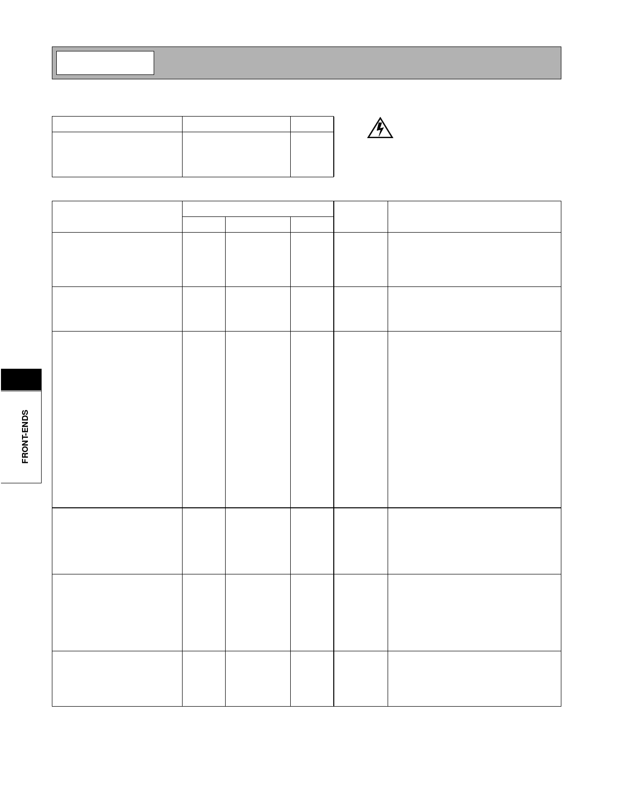
Absolute Maximum Ratings
Parameter
Supply Voltage
Input LO and RF Levels
Ambient Operating Temperature
Storage Temperature
Rating
-0.5 to 5.5
+6
-40 to +85
-40 to +150
Unit
VDC
dBm
°C
°C
Caution! ESD sensitive device.
RF Micro Devices believes the furnished information is correct and accurate
at the time of this printing. However, RF Micro Devices reserves the right to
make changes to its products without notice. RF Micro Devices does not
assume responsibility for the use of the described product(s).
Parameter
Overall
RF Frequency Range
LO Frequency Range
IF Frequency Range
Cascaded Performance
Cascade Conversion Gain
Cascade Input IP3
Cascade Noise Figure
First Section (LNA)
8
Noise Figure
Input VSWR
Input IP3
Gain
Reverse Isolation
Output VSWR
Second Section (Mixer)
Noise Figure
Input VSWR
Input IP3
Conversion Gain
Output Impedance
LO Input
LO Input Range
LO Output Level
LO to RF (Mix In) Rejection
LO to IF1, IF2 Rejection
LO Input VSWR
Power Supply
Voltage
Current Consumption
Specification
Min.
Typ.
Max.
1500
1200
DC
2500
2500
500
24
27
28
-17
-16
3.6
1.8
1.5:1
+4
2.0:1
+8.5
13.5
23
<1.5:1
10
1.5:1
-5
16
1
-3
+3
-7
-3
+1
-22
-14
30
20
1.5:1
2.7
3.6
5.0
7
52
48
Unit
MHz
MHz
MHz
dB
dBm
dB
dB
dBm
dBm
dB
dB
dB
dBm
dB
kΩ
dBm
dBm
dBm
dB
dB
V
mA
mA
mA
Condition
T = 25°C, VCC=3.6V, RF=1959MHz,
LO=1749MHz @ +1 dBm
1kΩ balanced load, 2.5dB Image Filter Loss.
Single Sideband
The LNA section may be left unused. Power
is not connected to pin 1. The performance
is then as specified for the Second Section
(Mixer).
Input is internally matched for optimum noise
figure from a 50Ω source.
IP3 may be increased 10dB by connecting
pin 22 to VCC through the matching inductor.
The LNA’s current then increases by 10mA.
Other in-between IP3 versus ICC trade-offs
may be made. See pin description for pin 20.
R2 = Open
R2 = Short
With 1kΩ balanced load.
Single Sideband
Balanced
Buffer On, +1dBm input
Buffer Off, +1dBm input
Single ended
LNA only
LNA + Mixer, LO Buffer On
LNA + Mixer, LO Buffer Off
8-106
Rev A7 010717
Share Link: 