LTC1456IN8 Ver la hoja de datos (PDF) - Linear Technology
Número de pieza
componentes Descripción
Lista de partido
LTC1456IN8 Datasheet PDF : 8 Pages
| |||
U
OPERATIO
Serial Interface
The data on the DIN input is loaded into the shift register
on the rising edge of the clock. The MSB is loaded first. The
DAC register loads the data from the shift register when
CS/LD is pulled high. The CLK is disabled internally when
CS/LD is high. Note: CLK must be low before CS/LD is
pulled low to avoid an extra internal clock pulse.
When CLR is pulled low it asynchronously resets the shift
and DAC registers to all zeros.
The buffered output of the 12-bit shift register is available
on the DOUT pin which swings from GND to VCC. Multiple
LTC1456s may be daisy-chained together by connecting
the DOUT pin to the DIN pin of the next chip, while the CLK
LTC1456
and CS/LD signals remain common to all chips in the daisy
chain. The serial data is clocked to all of the chips, then the
CS/LD signal is pulled high to update all of them simulta-
neously.
Voltage Output
The LTC1456's rail-to-rail buffered output can source or
sink 5mA over the entire operating temperature range
while pulling to within 300mV of the positive supply
voltage or ground. The output swings to within a few
millivolts of either supply rail when unloaded and has an
equivalent output resistance of 40Ω when driving a load to
the rails. The output can drive 1000pF without going into
oscillation.
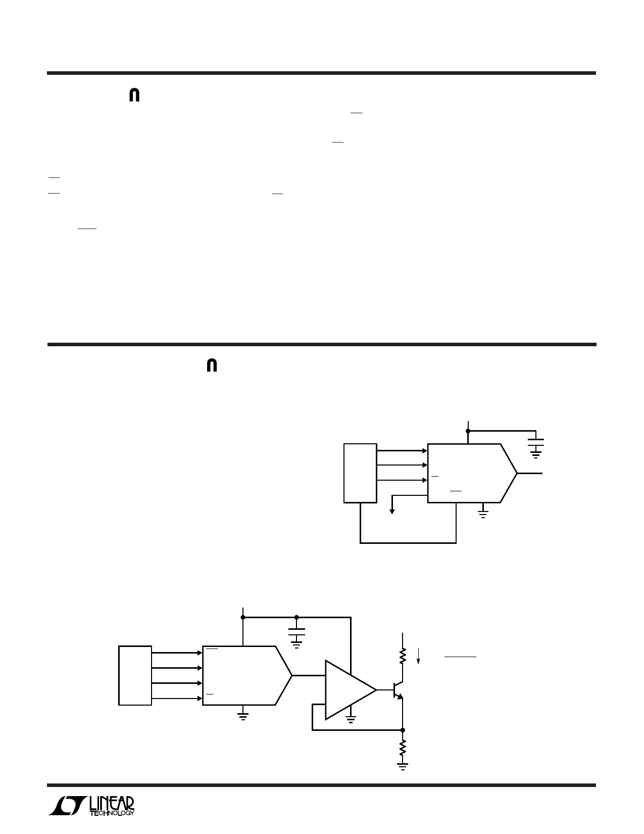
TYPICAL APPLICATION
The circuit below shows a digitally programmable current
source from an external voltage source using an external
op amp, an LT®1077 and an NPN transistor (2N3440). Any
digital word from 0 to 4095 is loaded into the LTC1456 and
its output correspondingly swings from 0V to 4.095V. In
the configuration shown, this voltage will be forced across
the resistor RA. If RA is chosen to be 410Ω the output
current will range from 0mA at zero scale to 10mA at full
scale. The minimum voltage for VS is determined by the
load resistor RL and Q1’s VCESAT voltage. With a load
resistor of 50Ω, the voltage source can be as low as 5V.
12-Bit 5V Single Supply Voltage Output DAC
4.5V TO 5.5V
DIN
VCC
CLK
µP
LTC1456 VOUT
CS/LD
DOUT CLR GND
TO NEXT DAC FOR
DAISY-CHAINING
0.1µF
OUTPUT
0V TO 4.095V
1456 TA03
Digitally Programmable Current Source
5V
0.1µF
VS + 5V TO 100V
FOR RL ≤ 50Ω
CLR
VCC
µP
CLK
LTC1456 VOUT
+
RL
IOUT
=
DIN • 4.095
4096 • RA
≈
0mA
TO
10mA
DIN
CS/LD GND
LT1077
–
Q1
2N3440
RA
410Ω
1456 TA04
Information furnished by Linear Technology Corporation is believed to be accurate and reliable.
However, no responsibility is assumed for its use. Linear Technology Corporation makes no represen-
tation that the interconnection of its circuits as described herein will not infringe on existing patent rights.
7
Share Link: 