LT1641IS8 Ver la hoja de datos (PDF) - Linear Technology
Número de pieza
componentes Descripción
Lista de partido
LT1641IS8 Datasheet PDF : 12 Pages
| |||
LT1641
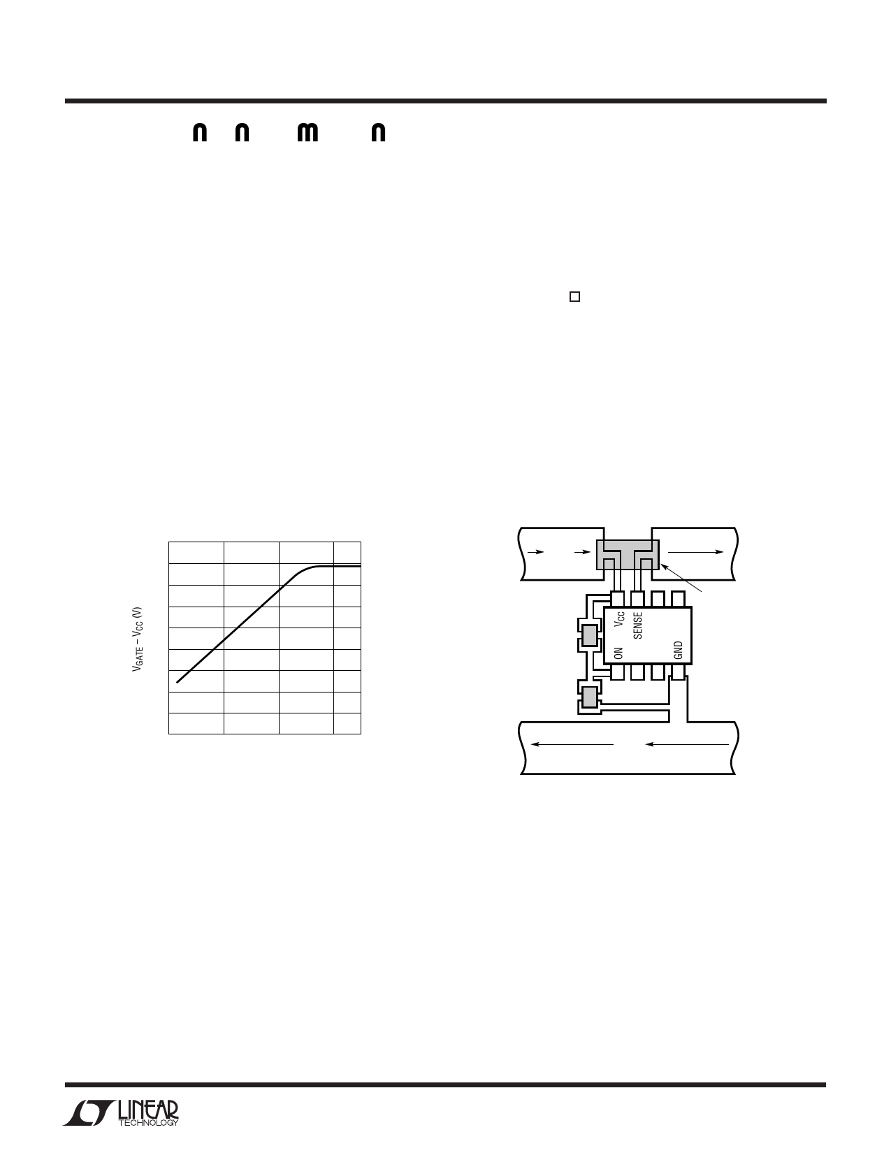
APPLICATIO S I FOR ATIO
GATE Pin Voltage
A curve of gate drive vs VCC is shown in Figure 15. The
GATE pin is clamped to a maximum voltage of 18V above
the input voltage. At minimum input supply voltage of 9V,
the minimum gate drive voltage is 4.5V. When the input
supply voltage is higher than 20V, the gate drive voltage is
at least 10V and a regular N-FET can be used. In applica-
tions ranges 9V to 24V range, a logic level N-FET must be
used with a proper protection Zener diode between its gate
and source (as D1 shown is Figure 5).
Layout Considerations
To achieve accurate current sensing, a Kelvin connection
is recommended. The minimum trace width for 1oz cop-
per foil is 0.02" per amp to make sure the trace stays at a
reasonable temperature. 0.03" per amp or wider is recom-
mended. Note that 1oz copper exhibits a sheet resistance
of about 530µΩ/ . Small resistances add up quickly in
high current applications. To make the system immune to
noise, the resistor divider to the ON pin needs to be close
to the chip and keep traces to VCC and GND short. A 0.1µF
capacitor from the ON pin to GND also helps reject induced
noise. Figure 16 shows a layout that addresses these
issues.
18
16
14
12
10
8
6
4
2
0
8
13
18
VCC (V)
23
1641 F15
Figure 15. Gate Drive vs Supply Voltage
ILOAD
R1
LT1641
SENSE
RESISTOR, RS
R2
ILOAD
1541 F16
Figure 16. Recommended Layout for R1, R2 and RS
11
Share Link: 