AD7545AN(1997) Ver la hoja de datos (PDF) - Intersil
Número de pieza
componentes Descripción
Lista de partido
AD7545AN Datasheet PDF : 7 Pages
| |||
AD7545
Absolute Maximum Ratings
Supply Voltage (VDD to DGND) . . . . . . . . . . . . . . . . . . . -0.3V, +17V
Digital Input Voltage to DGND . . . . . . . . . . . . . . . .-0.3V, VDD +0.3V
VRFB, VREF to DGND . . . . . . . . . . . . . . . . . . . . . . . . . . . . . . . ±25V
VPIN1 to DGND . . . . . . . . . . . . . . . . . . . . . . . . . . .-0.3V, VDD +0.3V
AGND to DGND . . . . . . . . . . . . . . . . . . . . . . . . . . .-0.3V, VDD +0.3V
Operating Conditions
Thermal Information
Thermal Resistance (Typical, Note 1)
θJA (oC/W)
PDIP Package . . . . . . . . . . . . . . . . . . . . . . . . . . . . .
125
Maximum Junction Temperature (PDIP Package) . . . . . . . . . 150oC
Maximum Storage Temperature Range . . . . . . . . . .-65oC to 150oC
Maximum Lead Temperature (Soldering 10s) . . . . . . . . . . . . 300oC
Temperature Ranges
Commercial (J, K, Grades) . . . . . . . . . . . . . . . . . . . . .0oC to 70oC
Industrial (A, B, Grades) . . . . . . . . . . . . . . . . . . . . . -40oC to 85oC
Extended (S Grades) . . . . . . . . . . . . . . . . . . . . . . -55oC to 125oC
CAUTION: Stresses above those listed in “Absolute Maximum Ratings” may cause permanent damage to the device. This is a stress only rating and operation
of the device at these or any other conditions above those indicated in the operational sections of this specification is not implied.
NOTE:
1. θJA is measured with the component mounted on an evaluation PC board in free air.
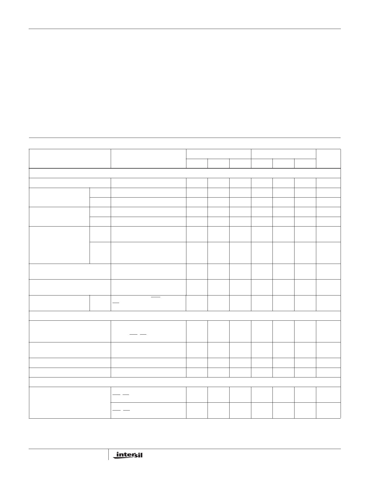
Electrical Specifications TA = See Note 2, VREF = +10V, VOUT1 = 0V, AGND = DGND, Unless Otherwise Specified
PARAMETER
TEST CONDITIONS
VDD = +5V
MIN TYP MAX
STATIC PERFORMANCE
Resolution
12
Relative Accuracy
J, A, S
-
-
±2
K, B
-
-
±1
Differential Nonlinearity J, A, S 10-Bit Monotonic TMIN to TMAX
-
K, B 12-Bit Monotonic TMIN to TMAX
-
Gain Error
J, A, S DAC Register Loaded with
-
(Using Internal RFB)
1111 1111 1111
-
±4
-
±1
-
±20
K, B Gain Error is Adjustable
Using the Circuits of
Figures 4 and 5 (Note 3)
-
-
±10
Gain Temperature Coefficient
Typical Value is 2ppm/oC for
-
-
±5
∆Gain/∆Temperature
VDD = +5V (Note 4)
DC Supply Rejection
∆Gain/∆VDD
∆VDD = ±5%
0.015
-
0.03
Output Leakage Current
at OUT1
J, K DB0 - DB11 = 0V; WR,
A, B CS = 0V (Note 2)
-
-
50
-
-
50
S
-
-
200
DYNAMIC CHARACTERISTICS
Current Setting Time
To 1/2 LSB, OUT1 LOAD = 100Ω, -
-
2
DAC Output Measured from
Falling Edge of WR, CS = 0V
(Note 4)
Propagation Delay from Digital Input OUT1 LOAD = 100Ω,
-
Change to 90% of Final Analog
CEXT = 13pF (Notes 4 and 5)
Output
-
300
Digital to Analog Glitch Impulse
AC Feedthrough at OUT1
VREF = AGND
VREF = ±10V, 10kHz Sinewave
(Note 6)
-
400
-
-
5
-
ANALOG OUTPUTS
Output Capacitance
COUT1
DB0 - DB11 = 0V,
WR, CS = 0V (Note 4)
-
-
70
COUT1
DB0 - DB11 = VDD,
WR, CS = 0V (Note 4)
-
-
200
VDD = +15V
MIN TYP MAX
UNITS
12
Bits
-
-
±2
LSB
-
-
±1
LSB
-
-
±4
LSB
-
-
±1
LSB
-
-
±25
LSB
-
-
±15
LSB
-
-
±10 ppm/oC
0.01
-
0.02
%
-
-
50
nA
-
-
50
nA
-
-
200
nA
-
-
2
µs
-
-
250
ns
-
250
-
nV/s
-
5
-
mVP-P
-
-
70
pF
-
-
200
pF
10-11
Share Link: 