AD642JH Ver la hoja de datos (PDF) - Analog Devices
Número de pieza
componentes Descripción
Lista de partido
AD642JH Datasheet PDF : 6 Pages
| |||
AD642–SPECIFICATIONS (@ + 25°C, and VS = ±15 V dc)
Model
AD642J
AD642K
Min Typ
Max Min Typ Max
AD642L
AD642S
Min Typ Max Min Typ Max Unit
OPEN LOOP GAIN
VO = ± 10 V, RL ≥ 2 kΩ
TMIN to TMAX, RL = 2 kΩ
OUTPUT CHARACTERISTICS
Voltage @ RL = 2 kΩ, TMIN to TMAX
Voltage @ RL = 10 kΩ, TMIN to TMAX
Short Circuit Current
100,000
100,000
±10
± 12
±12
± 13
25
250,000
250,000
±10
± 12
±12
± 13
25
250,000
250,000
±10
± 12
±12
± 13
25
250,000
V/V
100,000
V/V
±10
± 12
V
±12
± 13
V
25
mA
FREQUENCY RESPONSE
Unity Gain Small Signal
Full Power Response
Slew Rate, Unity Gain
INPUT OFFSET VOLTAGE1
Initial Offset
Input Offset Voltage TMIN to TMAX
Input Offset Voltage vs. Supply,
TMIN to TMAX
INPUT BIAS CURRENT2
Either Input
Offset Current
1.0
50
2.0
3.0
10
5
1.0
50
2.0
3.0
2.0
1.0
3.5
2.0
200
100
75
10
35
2
1.0
50
2.0
3.0
1.0
50
2.0
3.0
MHz
kHz
V/µs
0.5
1.0 mV
1.0
3.5 mV
100
100 µV/V
10
35
2
10
35 pA
2
MATCHING CHARACTERISTICS3
Input Offset Voltage
Input Offset Voltage TMIN to TMAX
Input Bias Current
Crosstalk
1.0
3.5
35
–124
0.5
2.0
25
–124
0.25
1.0
25
–124
0.5 mV
3.5 mV
35 pA
–124
dB
INPUT IMPEDANCE
Differential
Common Mode
1012ʈ6
1012ʈ6
1012ʈ6
1012ʈ6
1012ʈ6
1012ʈ6
1012ʈ6
1012ʈ6
MΩʈpF
MΩʈpF
INPUT VOLTAGE RANGE
Differential4
Common Mode
Common-Mode Rejection
± 20
±10
± 12
76
± 20
±10
± 12
80
± 20
±10
± 12
80
± 20
V
±10
± 12
V
80
dB
INPUT NOISE
Voltage 0.1 Hz to 10 Hz
2
2
f = 10 Hz
70
70
f = 100 Hz
45
45
f = 1 kHz
30
30
f = 10 kHz
25
25
2
2
µV p-p
70
70
nV/√Hz
45
45
nV/√Hz
30
30
nV/√Hz
25
25
nV/√Hz
POWER SUPPLY
Rated Performance
Operating
Quiescent Current
± 15
± 15
±5
± 18 ± 5
± 15
2.8
2.8
± 15
± 15
V
±5
± 15
±5
± 15 V
2.8
2.8 mA
TRANSISTOR COUNT
58
58
58
58
PACKAGE OPTION
TO-99 Style (H-08B)
AD642JH
AD642KH
AD642LH
AD642SH
NOTES
1Input Offset Voltage specifications are guaranteed after 5 minutes of operation at T A = +25°C.
2Bias Current specifications are guaranteed at maximum at either input after 5 minutes of operation at T A = +25°C. For higher temperatures, the current doublers
every 10°C.
3Matching is defined as ther difference between parameters of the two amplifiers.
4Defined as the maximum safe voltage between inputs, such that neither exceeds ± 10 V from ground.
Specifications subject to change without notice.
Specifications shown in boldface are tested on all production units at final electrical test. Results from those tests are used to calculate outgoing quality levels. All min
and max specifications are guaranteed, although only those shown in boldface are tested on all production units.
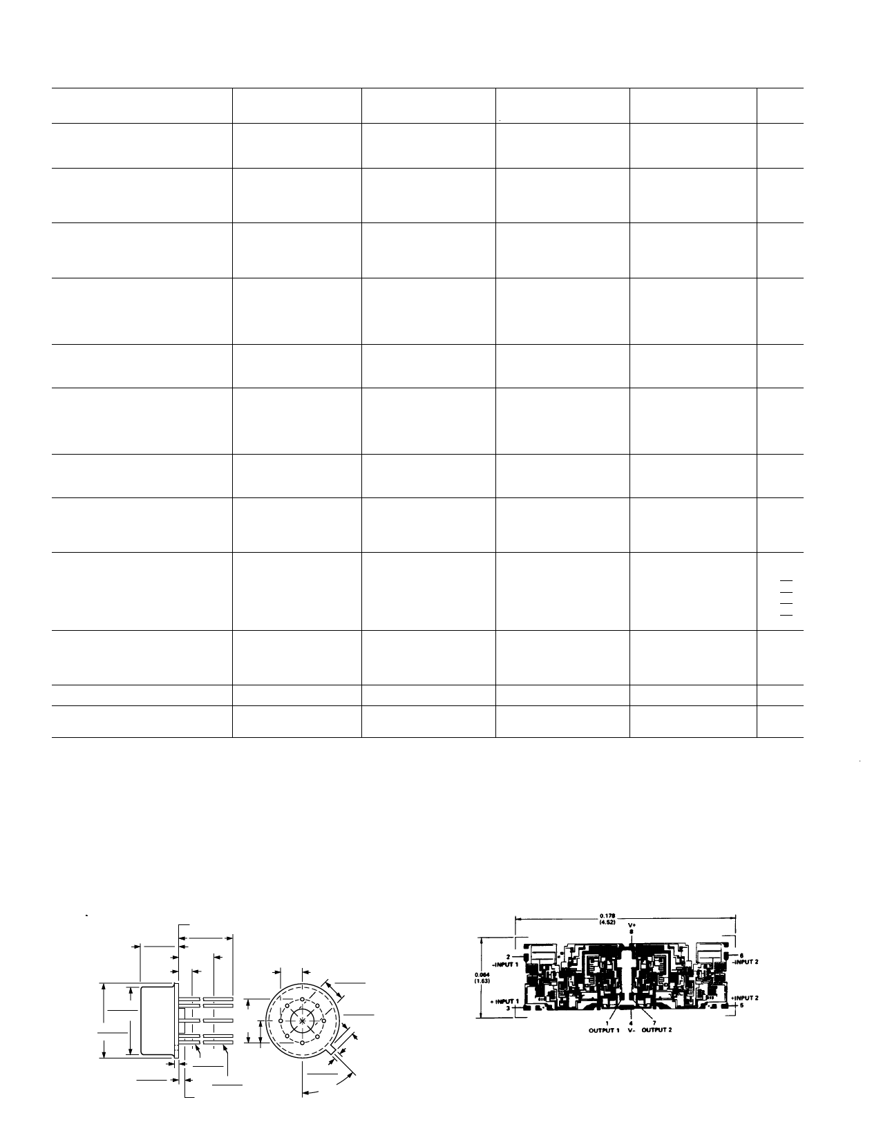
OUTLINE DIMENSIONS
Dimensions shown in inches and (mm).
TO-99
METALIZATION PHOTOGRAPHIC
Contact factory for latest dimensions.
Dimensions shown in inches and (mm).
0.185 (4.70)
0.165 (4.19)
0.050
(1.27)
MAX
REFERENCE PLANE
0.750 (19.05)
0.500 (12.70)
0.250 (6.35)
MIN
0.100
(2.54)
BSC
5
0.160 (4.06)
0.110 (2.79)
0.335 (8.51)
0.305 (7.75)
0.370 (9.40)
0.335 (8.51)
4
0.200
(5.08)
3
BSC
2
6
0.045 (1.14)
7 0.027 (0.69)
8
0.040 (1.02) MAX
0.045 (1.14)
0.010 (0.25)
0.019 (0.48)
0.016 (0.41)
0.100
(2.54)
BSC
0.021 (0.53)
0.016 (0.41)
BASE & SEATING PLANE
1
0.034 (0.86)
0.027 (0.69)
45°
BSC
–2–
REV. 0
Share Link: 