5962R9676601QXC Ver la hoja de datos (PDF) - Intersil
Número de pieza
componentes Descripción
Lista de partido
5962R9676601QXC Datasheet PDF : 11 Pages
| |||
HS-81C55RH, HS-81C56RH
HS-81C55RH AND HS-81C56RH
ONE BIT OF PORT A OR PORT B
OUTPUT
D LATCH Q
CLK CLR
(1) OUTPUT MODE
(2) SIMPLE INPUT
(3) STROBED INPUT
MULTIPLEXER
CONTROL
(4) = 1 FOR OUTPUT MODE
= 0 FOR INPUT MODE
PA/PB
PIN
WRITE
PORT
MUX (1)
(2)
MODE (4)
READ
PORT
(3)
LATCH
Q
D
CLK
NOTES:
1. READ Port = (IO/M = 1)(RD = 0)(CE Active)
(Port Address Selected)
2. WRITE Port = (IO/M = 1)(wr = 0)(CE Active)
(Port Address Selected)
STB
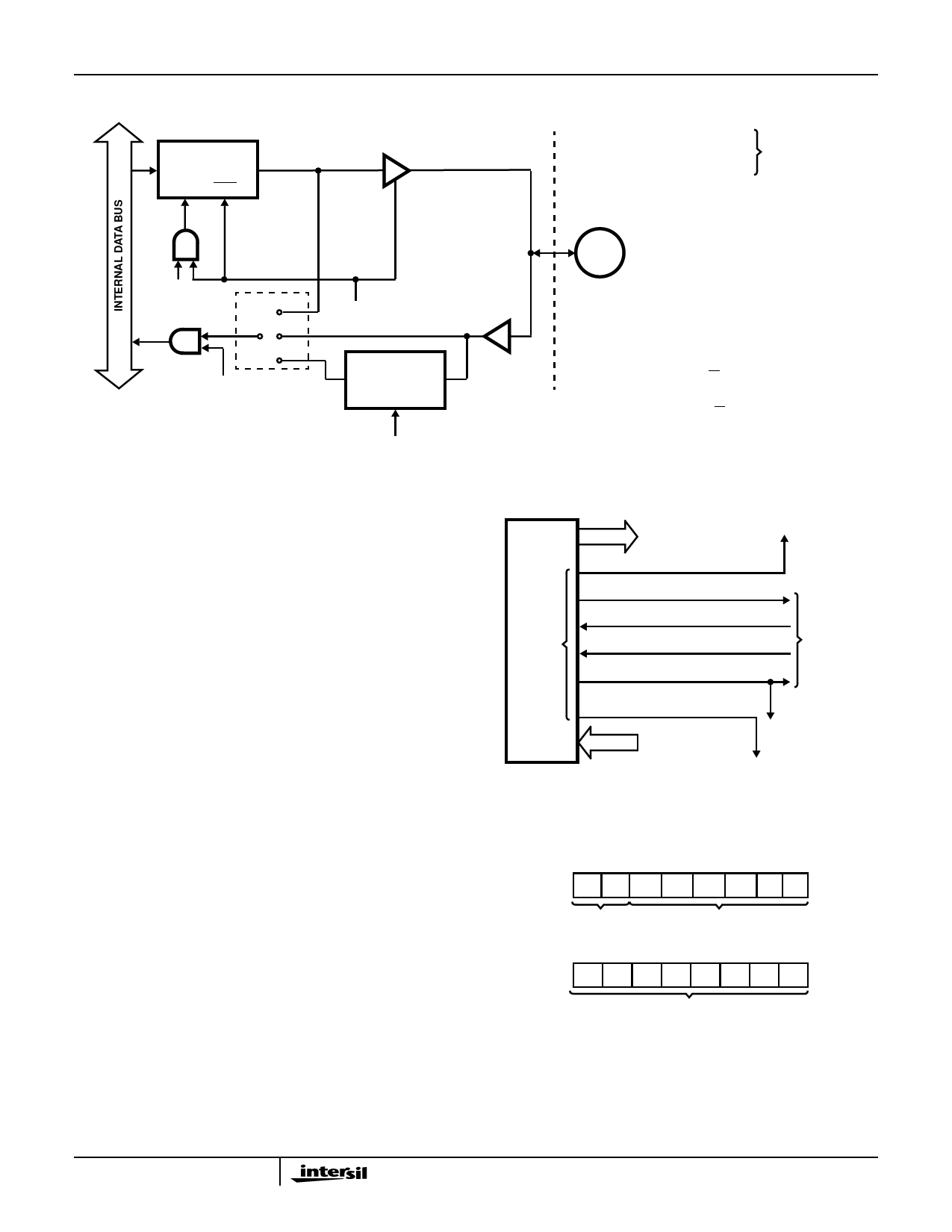
FIGURE 6. HS-81C55RH AND HS-81C56RH PORT FUNCTION
Figure 7 shows how the HS-81C55/56RH I/O ports might be
configured in a typical system.
Timer Section
The timer is a 14-bit down counter that counts the TIMER IN
pulses and provides either a square wave or pulse when
terminal count (TC) is reached.
The timer has the I/O address XXXXX100 for the low order
byte of the register and the I/O address XXXXX101 for the
high order byte of the register. (See Figure 5).
To program the timer, the COUNT LENGTH REG is loaded
first, one byte at a time, by selecting the timer addresses.
Bits 0-13 of the high order count register will specify the
length of the next count and bits 14-15 of the high order
register will specify the timer output mode (see Figure 8).
The value loaded into the count length register can have any
value from 2H through 3FFH in Bits 0-13.
PORT A OUTPUT PORT A
TO HS-80C85RH
RST INPUT
A INTR (SIGNAL DATA RECEIVED)
A BF (SIGNALS DATA READY)
PORT C
A STB (ACKNOWL. DATA RCV’D)
B STB (LOAD PORT B LATCH)
B BF (SIGNALS BUFFER IS FULL)
TO/FROM
PERIPHERAL
INTERFACE
PORT B
B INTR (SIGNALS BUFFER
READY FOR READING)
INPUT
TO INPUT PORT
(OPTIONAL)
TO HS-80C85RH
RST INPUT
FIGURE 7. EXAMPLE: COMMAND REGISTER = 00111001
76543210
M2 M1 T13 T12 T11 T10 T9 T8
TIMER
MODE
MSB OF
CNT LENGTH
76543210
T7 T6 T5 T4 T3 T2 T1 T0
LSB OF
CNT LENGTH
FIGURE 8. TIMER FORMAT
There are four modes to choose from: M2 and M1 define the
timer mode, as shown in Figure 9.
9
Share Link: 