RF2667PCBA Ver la hoja de datos (PDF) - RF Micro Devices
Número de pieza
componentes Descripción
Lista de partido
RF2667PCBA Datasheet PDF : 10 Pages
| |||
RF2667
Pin Function Description
Interface Schematic
14
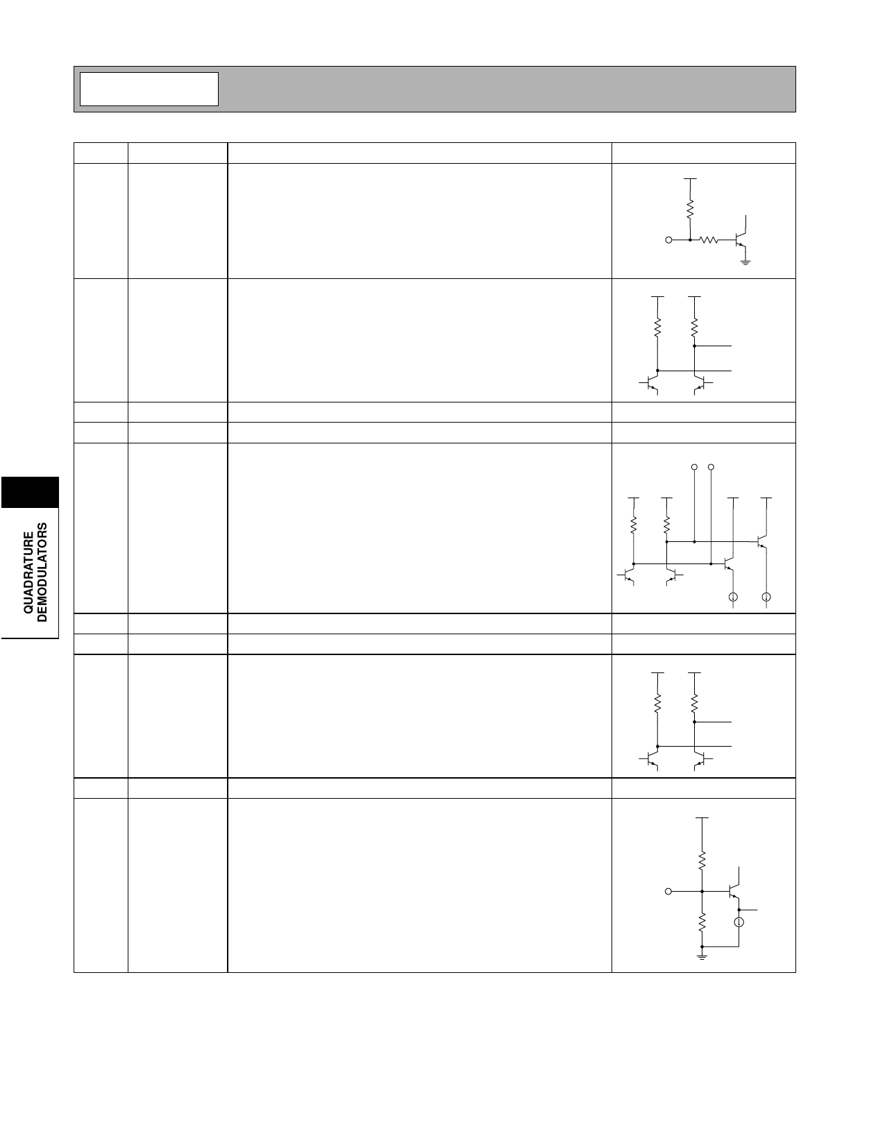
IN SEL
Selects between CDMA and FM mode. This is a digitally controlled
input. A logic “high” (≥VCC-0.7VDC) selects CDMA mode. A logic “low”
(<0.5VDC) selects FM mode. The impedance on this pin is 30kΩ.
BIAS
60 kΩ
IN SEL
60 kΩ
15
Q OUT- Balanced Baseband Output of Q Mixer. This pin is internally DC biased
and should be DC blocked externally. This output is active in both
CDMA and FM modes. The output can be used in a single-ended con-
figuration by leaving one of the two pins unconnected, however half the
output voltage will be lost. Each pin should be loaded with 2.5kΩ. The
balanced load should be 5kΩ. The single-ended output impedance is
1.2kΩ, while the balanced output impedance is 2.4kΩ.
VCC
VCC
1.2 kΩ 1.2 kΩ
Q OUT+
Q OUT-
16
Q OUT+ Same as pin 15, except complementary output.
See pin 15.
17
GND
Same as pin 6.
18
7
FL-
Balanced AGC Output/Demod Input. This balanced node is pinned out
to allow shunt filtering of the AGC output signal as it enters the demod-
ulator. The basic configuration of the filter should consist of a shunt
inductor and shunt capacitor, both connected to the power supply, as
the internal circuitry requires this power supply connection through the
inductor to operate.
FL- FL+
VCC2
VCC2
1.2 kΩ 1.2 kΩ
VCC1
VCC1
19
FL+
Same as pin 18, except complementary.
See pin 18.
20
GND
Same as pin 6.
21
I OUT+
Balanced Baseband Output of I Mixer. This pin is internally DC biased
and should be DC blocked externally. This output is active in both
CDMA and FM modes. The output can be used in a single-ended con-
figuration by leaving one of the two pins unconnected, however half the
output voltage will be lost. Each pin should be loaded with 2.5kΩ. The
balanced load should be 5kΩ. The single-ended output impedance is
1.2kΩ, while the balanced output impedance is 2.4kΩ.
VCC
VCC
1.2 kΩ 1.2 kΩ
I OUT+
I OUT-
22
I OUT-
Same as pin 21, except complementary output.
See pin 22.
23
GC
Analog Gain Control for AGC Amplifiers. The valid control range is from
BIAS
0.5 to 2.5VDC. These voltages are valid for ONLY a 37kΩ source
impedance. The gain range for the AGC is 95dB.
21 kΩ
GC
40 kΩ
7-4
Rev A14 010622
Share Link: 