PI74SSTV16859(2000) Ver la hoja de datos (PDF) - Pericom Semiconductor
Número de pieza
componentes Descripción
Lista de partido
PI74SSTV16859 Datasheet PDF : 7 Pages
| |||
ADVANCE INFORMATION
PI74SSTV16859
13-Bit to 26-Bit Registered Buffer
1122334455667788990011223344556677889900112233445566778899001122112233445566778899001122334455667788990011223344556677889900112211223344556677889900112233445566778899001122334455667788990011221122334455667788990011223344556677889900112233445566778899001122112233445566778899001122
Truth Table(1)
Inputs
Outputs
RESET CLK
CLK
D
Q
L
X or
Floating
X or
Floating
X or
Floating
L
H
↑
↓
H
H
Η
↑
↓
L
L
H
L or H L or H
X
Qo(2)
Notes:
1. H = High Signal Level
L = Low Signal Level
↑ = Transition LOW-to-HIGH
↓ = Transition HIGH-to-LOW
X = Irrelevant or floating
2. Output level before the
indicated steady state
input conditions were
established.
Maximum Ratings (Above which the useful life may be
impaired. For user guidelines, not tested.)
Item
Symbol/
Conditions
Ratings Units
Storage temperature
Tstg
65 to 150 °C
Supply voltage
VDD or VDDQ 0.5 to 3.6
Input voltage(1,2)
VI
0.5 to VDD
+0.5
V
Output voltage(1,2)
VO
0.5 to
VDDQ +0.5
Input clamp current
IIK, VI <0
or VI >VDD
±50
Output clamp
current
IOK, VO <0
or VO >VDDQ
±50
mA
Continuous output
current
IO, VO = 0
to VDDQ
±50
VDD, VDDQ
or GND current/pin
IDD, IDDQ
or IGND
±100
Package Thermal
Impedance(3)
θJA
55
°C/W
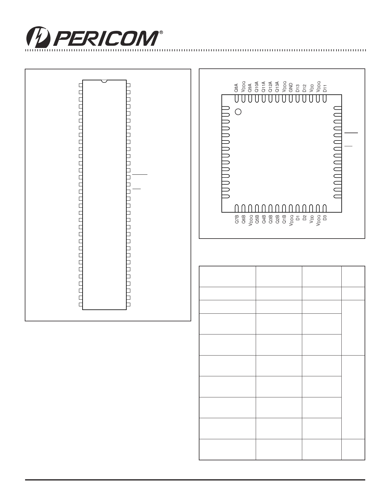
Product Pin Configuration
Q13A 1
64 VDDQ
Q12A 2
63 GND
Q11A 3
62 D13
Q10A 4
61 D12
Q9A 5
60 VDD
VDDQ 6
GND 7
59 VDDQ
58 GND
Q8A 8
57 D11
Q7A 9
56 D10
Q6A 10
55 D9
Q5A 11
54 GND
Q4A 12 64-Pin 53 D8
Q3A 13 A 52 D7
Q2A 14
51 RESET
GND 15
50 GND
Q1A 16
49 CK
Q13B 17
48 CK
VDDQ 18
47 VDDQ
Q12B 19
Q11B 20
46 VDD
45 VREF
Q10B 21
44 D6
Q9B 22
43 GND
Q8B 23
42 D5
Q7B 24
41 D4
Q6B 25
40 D3
GND 26
39 GND
VDDQ 27
Q5B 28
Q4B 29
38 VDDQ
37 VDD
36 D2
Q3B 30
35 D1
Q2B 31
34 GND
Q1B 32
33 VDDQ
Note:
Stresses greater than those listed under MAXIMUM RATINGS
may cause permanent damage to the device. This is a stress rating
only and functional operation of the device at these or any other
conditions above those indicated in the operational sections of this
specification is not implied. Exposure to absolute maximum rating
conditions for extended periods may affect reliability.
1. The input and output negative voltage ratings may be
excluded if the input and output clamp ratings are observed.
2. This value is limited to 3.6V Maximum.
3. The package thermal impedance is calculated in accordance
with JESD 51.
2
PXXXX 07/27/00
Share Link: 