CXG1068N Ver la hoja de datos (PDF) - Sony Semiconductor
Número de pieza
componentes Descripción
Lista de partido
CXG1068N Datasheet PDF : 6 Pages
| |||
CXG1068N
SP4T Antenna Switch for GSM Dual band
For the availability of this product, please contact the sales office.
Description
The CXG1068N is a high power antenna switch
MMIC for use in Dualband GSM handsets.
One antenna can be routed to either of the 2Tx or
2Rx ports. This IC is designed using the Sony’s
GaAs J-FET process which enable the CXG1068N
to be operated with low voltage.
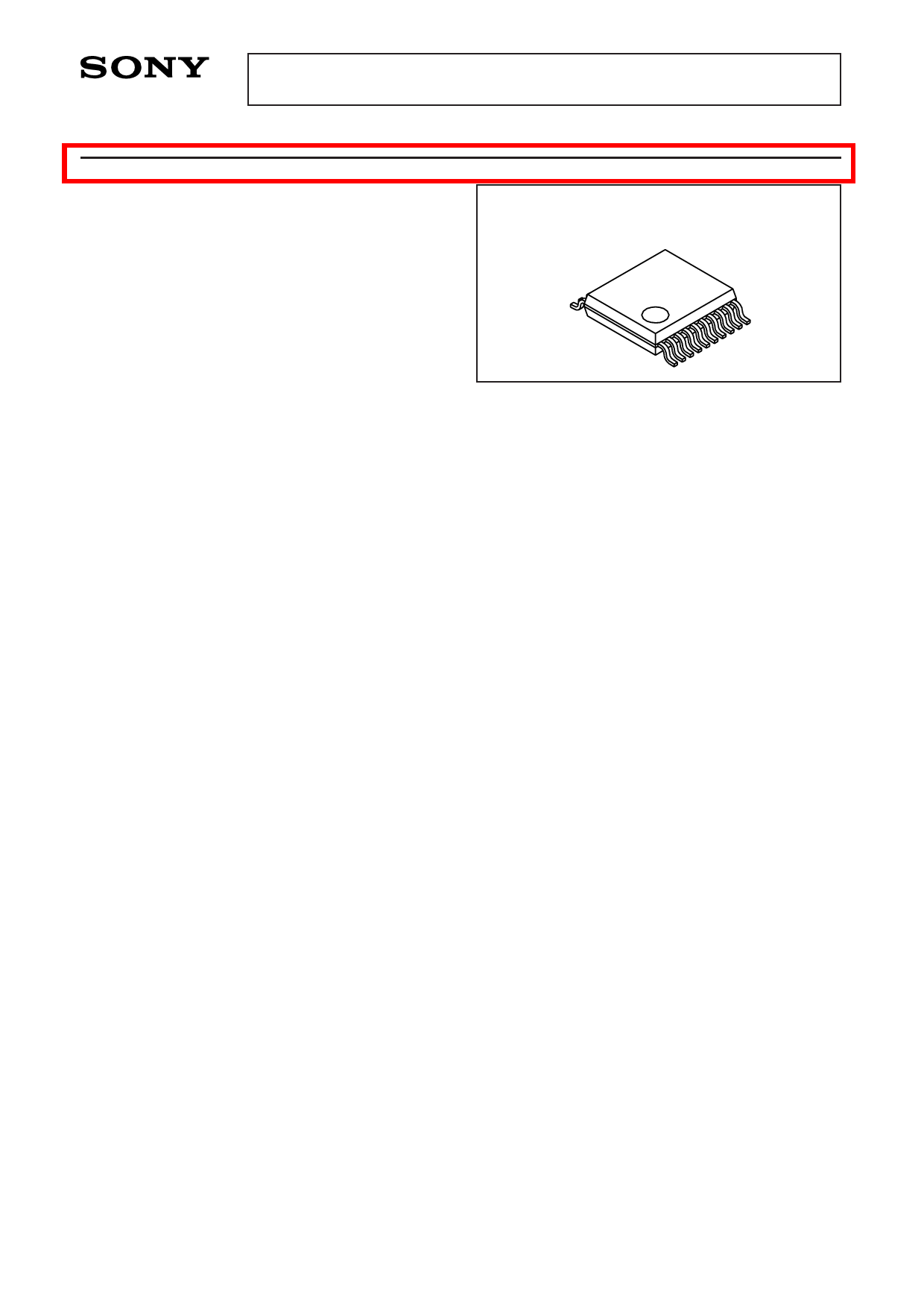
20 pin SSOP (Plastic)
Features
• Low control voltage
• Low insertion loss : 0.5 dB (Typ.) @900 MHz
0.65 dB (Typ.) @1.8 GHz
• Small package :
Operating Conditions (Ta=25 °C)
Control voltage
Vctl (H)–Vctl (L): 2.5 to 5
V
SSOP-20pin (Pin interval of 0.5 mm pitch)
• High power handling :
P1dB : 38 dBm (Typ.) 0/5 V control
• Harmonics :
–31 dBm (Max.) Pin=35 dBm, 0/5 V control
Applications
• Dualband GSM 900/GSM 1800 or GSM 900/GSM
1900 handsets.
• Dualmode GSM/DECT handsets.
Structure
GaAs J-FET MMIC
GaAs MMICs are ESD sensitive devices. Special handling precautions are required.
Sony reserves the right to change products and specifications without prior notice. This information does not convey any license by
any implication or otherwise under any patents or other right. Application circuits shown, if any, are typical examples illustrating the
operation of the devices. Sony cannot assume responsibility for any problems arising out of the use of these circuits.
—1—
E98920A8X-TE
Share Link: 