PI6C102-16BH Ver la hoja de datos (PDF) - Pericom Semiconductor
Número de pieza
componentes Descripción
Lista de partido
PI6C102-16BH Datasheet PDF : 12 Pages
| |||
PI6C102-16
Spread Spectrum Clock Synthesizer
for Mobile Pentium II 1122334455667788990011223344556677889900112233445566778899001122112233445566778899001122334455667788990011223344556677889900112211223344556677889900112233445566778899001122334455667788990011221122334455667788990011223344556677889900112233445566778899001122112233445566778899001122
Minimum and Maximum Expected Capacitive Loads
Clock
Min. Load Max. Load Units
Notes
CPU Clocks (HCLK)
10
20
1 device load, possible 2 loads
PCI Clocks (PCLK)
30
30
pF Meets PCI 2.1 requirements
REF, 48MHz
10
20
1 device load
Notes:
1. Maximum rise/fall times are guaranteed at maximum specified load for each type of output buffer.
2. Minimum rise/fall times are guaranteed at minimum specified load for each type of output buffer.
3. Rise/fall times are specified with pure capacitive load as shown. Testing is done with an
additional 500Ω resistor in parallel.
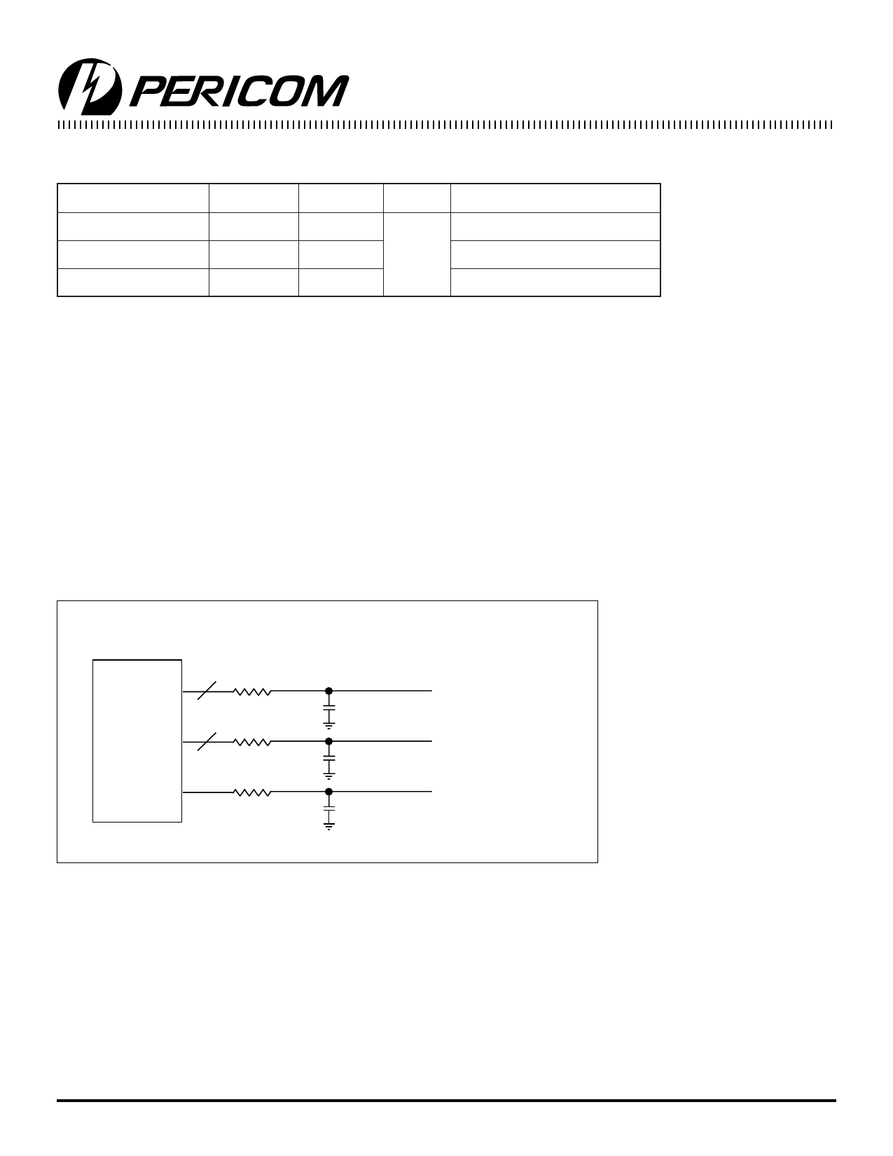
Design Guidelines to Reduce EMI
1. Place series resistors and CI capacitors as close as possible to the respective clock pins. Typical value
for CI is 10pF. Series resistor value can be increased to reduce EMI provided that the rise and fall time
are still within the specified values.
2. Minimize the number of “vias” of the clock traces.
3. Route clock traces over a continuous ground plane or over a continuous power plane. Avoid routing
clock traces from plane to plane (refer to rule #2).
4. Position clock signals away from signals that go to any cables or any external connectors.
PI6C102-16
2
CPUCLK
32Ω
6
33Ω
PCICLK
REF
22Ω/33Ω
CL
CL
CL
1 Device load
Meets PCI2.1 Req.
1 Device load
10
P8399-1 06/11/99
Share Link: 