M66235FP Ver la hoja de datos (PDF) - MITSUBISHI ELECTRIC
Número de pieza
componentes Descripción
Lista de partido
M66235FP Datasheet PDF : 5 Pages
| |||
MITSUBISHI 〈DIGITAL ASSP〉
M66235FP
STANDARD CLOCK GENERATOR
FUNCTION
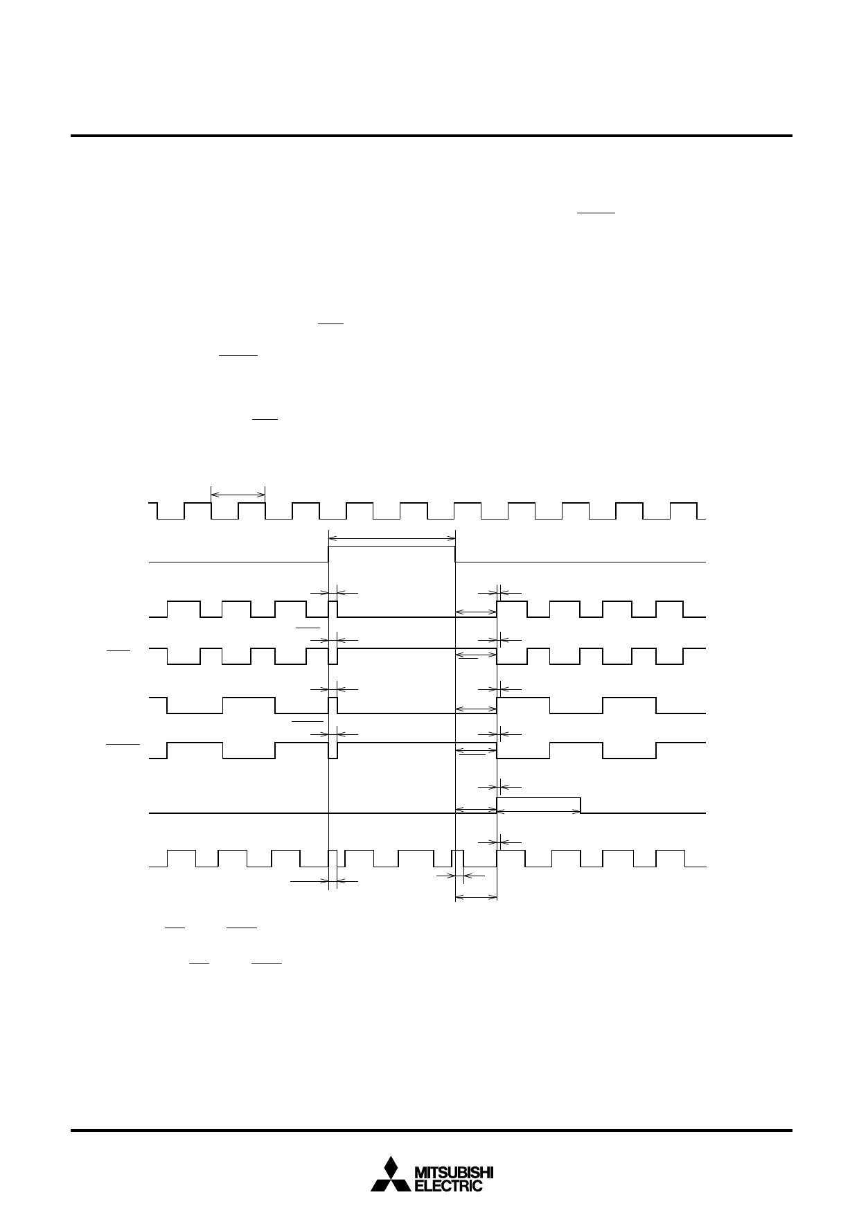
M66235 standard clock generator outputs clock input signal,
which is input to CLK IN, synchronously with optional trigger
signal, which is input to TR.
Sync clock output timing is determined by trigger input signal
fall edge. Time-lag between trigger input signal fall edge and
sync clock output equals the sum of clock input signal “L”
pulse width and M66235 internal delay. Variation in this lag
(∆t) is ±3ns, ensuring excellent synchronizing accuracy.
There are six types of outputs: synchronous clock output
(CKO), synchronous clock inverted output (CKO), 1/2 divider
synchronous clock output (CKO/2), 1/2 divider synchronous
clock inverted output (CKO/2), one-shot pulse output
(PULSE) and continuous clock output (CNTCK).
From synchronous clock output (CKO), sync clock of the
same frequency as clock input signal is output. From syn-
chronous clock inverted output (CKO), inverted signal of sync
clock output from CKO is output. From 1/2 divider synchro-
nous clock output (CKO/2), 1/2 divider signal of sync clock
output from CKO is output. From 1/2 divider synchronous
clock inverted output (CKO/2), inverted signal of that output
from CKO/2 is output.
From one-shot pulse output (PULSE), one-shot pulse which
is almost equal to two cycles of clock input signal is output
after trigger input signal falls. From continuous clock output
(CNTCK), sync clock is output when trigger input signal is on
“L” level; when trigger input signal is on “H” level, clock input
signal, which is input to CLK IN, is output.
All these outputs but continuous clock output are suspended
when trigger input signal is on “H” level: Synchronous clock
output, 1/2 divider synchronous clock output and one-shot
pulse output stay on “L” level, and synchronous clock inverted
output and 1/2 divider synchronous clock inverted output stay
on “H” level.
CLK IN
TR
CKO
CKO
CKO/2
CKO/2
PULSE
CNTCK
1/fIN
tsp(CKO)
tsp(CKO)
tsp(CKO/2)
tsp(CKO/2)
tCH
tw(TR)
∆t
tss (CKO)
∆t
tss(CKO)
∆t
tss(CKO/2)
∆t
tss(CKO/2)
tss(PULSE)
∆t
tw(PULSE)
∆t
tCL
tss(CNTCK)
VCC
0V
3V
0V
VOH
VOL
VOH
VOL
VOH
VOL
VOH
VOL
VOH
VOL
VOH
VOL
Note 1: tSS (CKO, CKO, CKO/2, CKO/2 and PULSE) equals the sum of input clock “L” width and α . Value α refers to internal delay in M66235. Under envi-
ronment where temperature and VCC do not change, value α and tss are kept constant. Dispersion of tss under such conditions is defined as ∆t [syn-
chronizing precision (jitter)].
Note 2: Outputs (CKO, CKO, CKO/2, CKO/2 PULSE and CNTCK) are unknown until trigger input TR reaches “H” level for the first time after power-on.
2
Share Link: 