AIC1782CS Ver la hoja de datos (PDF) - Analog Intergrations
Número de pieza
componentes Descripción
Lista de partido
AIC1782CS Datasheet PDF : 17 Pages
| |||
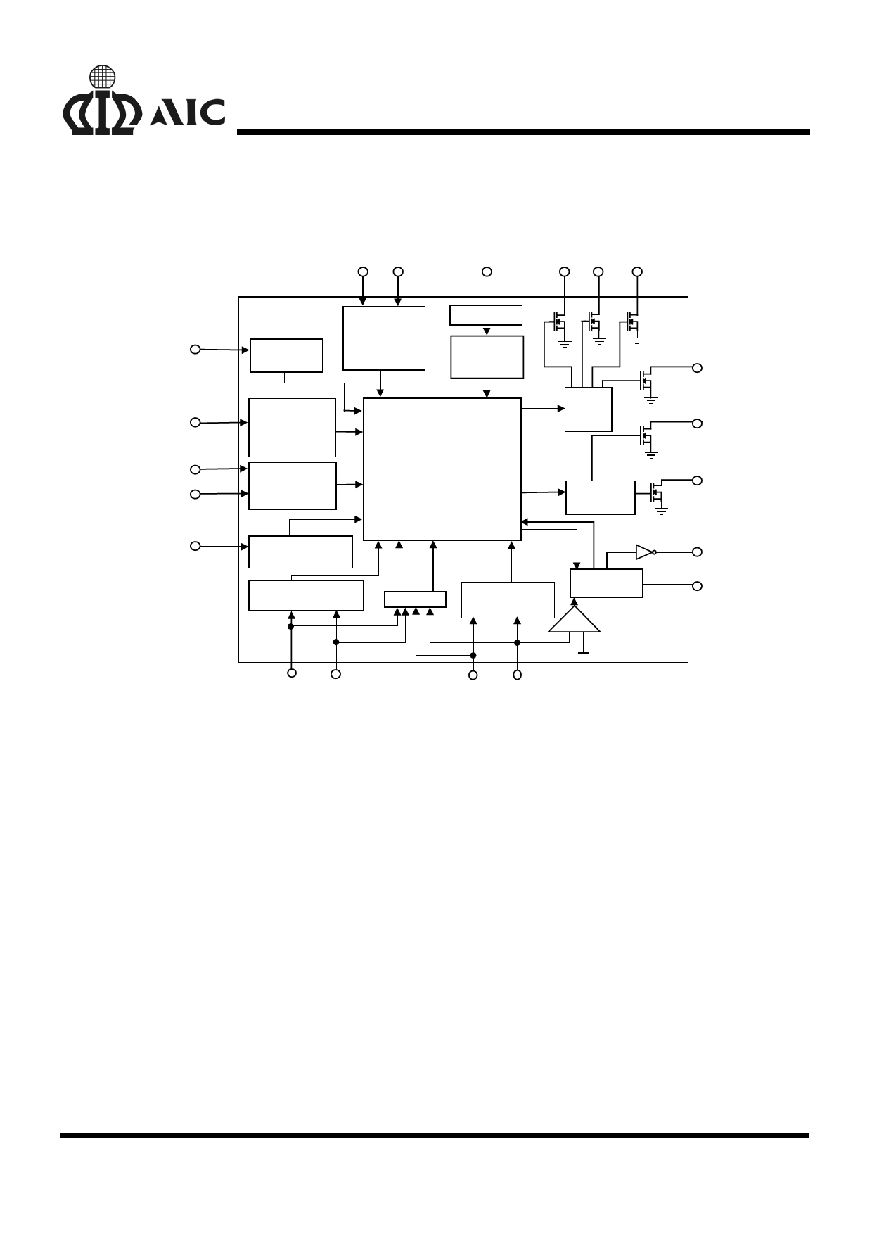
AIC1782
BLOCK DIAGRAM
GND VCC
TMR
LEB2 LEB1 LEA2
MODE
SEL3
SEL1
SEL2
ADJ
MODE
Selection
Bandgap
Reference
& Voltage
Regulator
Oscillator
Timing
Control Unit
Battery Voltage
& Temperature
Protection
Setting
LED Display&
Trickle Charge
Duty Setting
Charge Control
State Machine
Display
Control
Unit
Charge
Control Unit
∆T/∆t Detection
Setting
Battery Temperature
Protection
ATS BTS
13-bit A/D
Battery Voltage
Protection
Discharge
Control Unit
+-
CHARGE END
ABV BBV
LEA1
ICOB
ICOA
DIS
DSW
PIN DESCRIPTIONS
PIN 1: ABV - Divided battery voltage input to
sense the battery voltage of
pack A.
PIN 2: BBV - Divided battery voltage input to
sense the battery voltage of
pack B.
PIN 3: DIS
- Push-pull output, used to con-
trol an external transistor to dis-
charge the battery of pack B.
DIS is active high when function
of discharge is enabled.
PIN 4: BTS - The battery cell temperature of
pack B is represented as a volt-
age input to the AIC1782 at this
pin. The acceptable voltage
range of BTS pin is 0.29 VCC to
0.72 VCC.
PIN 5: VCC - Power supply input at 5V ±
10%.
PIN 6: ADJ
- For adjusting the slope of
∆T / ∆t . Acceptable voltage
range for this pin is approxi-
mately 0.28V to 3.8V. If volt-
age higher than VCC - 0.3V,
function of ∆T / ∆t detection is
disabled.
PIN 7: SEL3
- Determining the acceptable
voltage range of ABV and
BBV pins and mode of tem-
perature protection function.
7
Share Link: 