CS62180B-IP Ver la hoja de datos (PDF) - Cirrus Logic
Número de pieza
componentes Descripción
Lista de partido
CS62180B-IP Datasheet PDF : 52 Pages
| |||
CS62180A
CS62180B
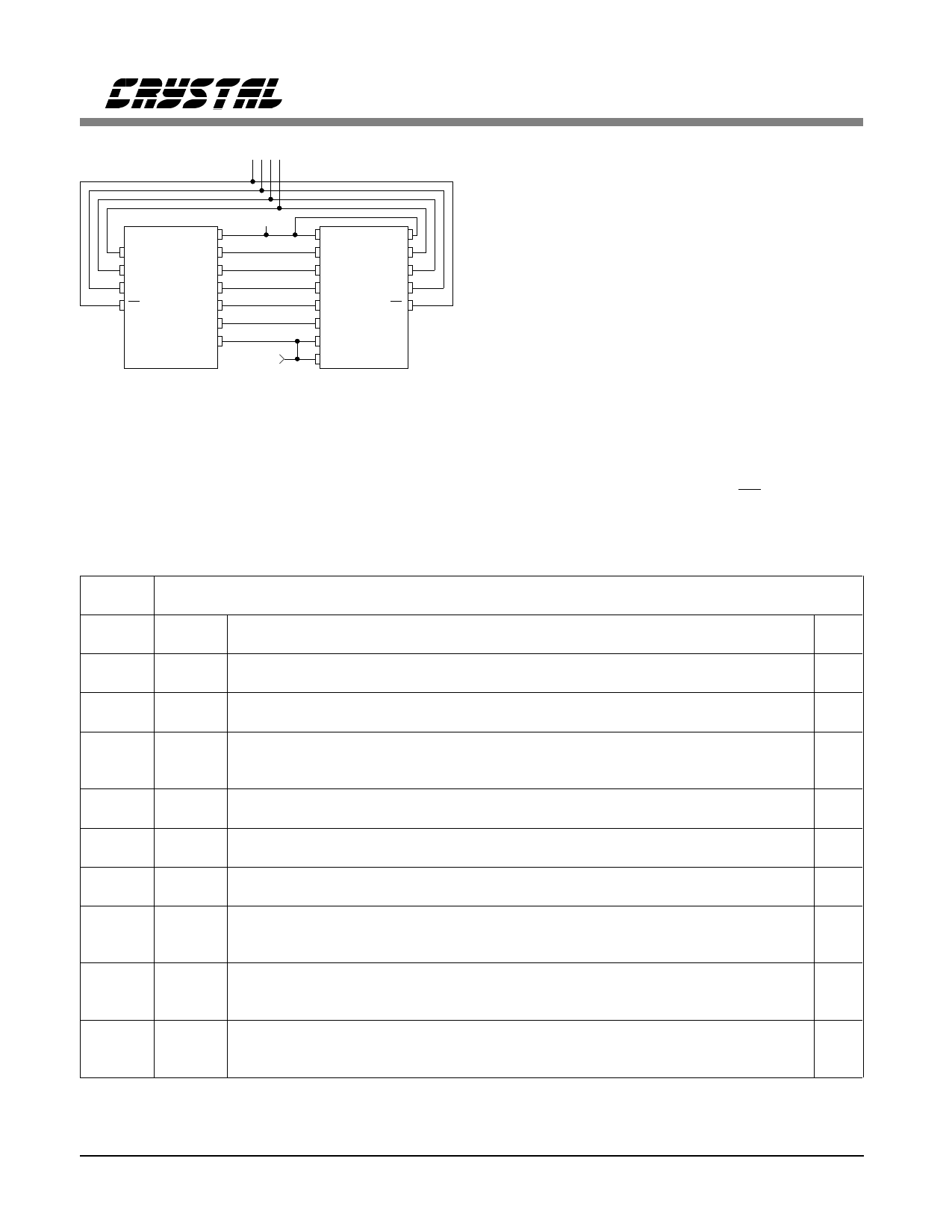
TO HOST CONTROLLER
SCLK
SDO
SDI
CS
SPS
TPOS
TNEG
RNEG
RPOS
RCLK
TCLK
CS62180A/B
V+
1.544 MHz
CLOCK
SIGNAL
MODE
CLKE
TPOS
SCLK
TNEG
SDO
RNEG
SDI
RPOS
CS
RCLK
TCLK
ACLKI
CS61535A
CS61574A or CS61575
Figure 3. Interfacing to a Crystal T1 LIU.
D7 (MSB) specifies burst mode if set to 1. When
using burst mode, the address field of the com-
mand word must be "0000", any other value will
invalidate the command, and the CS62180A and
CS62180B will simply ignore it. This effectively
means that the command for a burst write is 80
(hex) and a burst read is 81 (hex).
Burst mode allows the sixteen registers to be
consecutively read or written. Writing all regis-
ters allows fast initialization at power-up or
system reset. (Note that the Receiver Status Reg-
ister, RSR, is read-only, so a write during burst
mode will have no effect.) When using burst
mode, registers are read or written in address or-
der, 0000 (RSR) to 1111 (RMR3). Burst mode
ends on the first rising edge of CS. See Table 1
for a complete list of the CS62180A and
CS62180B on-chip registers.
ADDR
0000
0001
0010
0011
0100
0101
0110
0111
1000
1001
1010
1011
1100
1101
1110
1111
(T) TRANSMIT
REGISTER NAME AND DESCRIPTION
(R) RECEIVE
RSR Receive Status Register - A read only register which reports all active receiver
R
alarm conditions.
RIMR Receive Interrupt Mask Register - A mask which allows selection of individual
R
alarm conditions for generation of hardware interrupt.
BVCR Bipolar Violation Count Register - A bipolar violation alarm is generated after
R
this 8 bit counter surpasses it’s user definable limit.
ECR Error Count Register - Two separate 4 bit counters, which record OOF errors,
R
and frame bit or CRC errors. Like BVCR, each can be preset to a saturation
point.
CCR Common Control Register - Selects global configuration options, such as:
T/R
framing mode, zero suppression, or loopback.
RCR Receive Control Register - Selects receiver specific options, such as the resync R
algorithm or insertion of digital milliwatt codes.
TCR Transmit Control Register - Selects transmitter specific options, such as alarm
T
generation, clear or idle channel enable, and external S-bit or CRC insertion.
TIR1 Transmit Idle Registers - Each bit of the three TIR registers corresponds to an
T
TIR2
individual DS0 channel. When set, that channel is replaced with an idle code.
TIR3
TTR1 Transmit Transparent Registers - Each bit corresponds to a DS0 channel. When T
TTR2
set, that signaling and B7 zero suppression is disabled for that channel.
TTR3
RMR1 Receive Mark Registers - Each bit corresponds to a DS0 channel. When set, the R
RMR2
channel data is replaced with an idle or digital milliwatt code.
RMR3
Table 1. On-Chip Registers
DS225PP1
9
Share Link: 