MC145745FW Ver la hoja de datos (PDF) - Motorola => Freescale
Número de pieza
componentes Descripción
Lista de partido
MC145745FW Datasheet PDF : 16 Pages
| |||
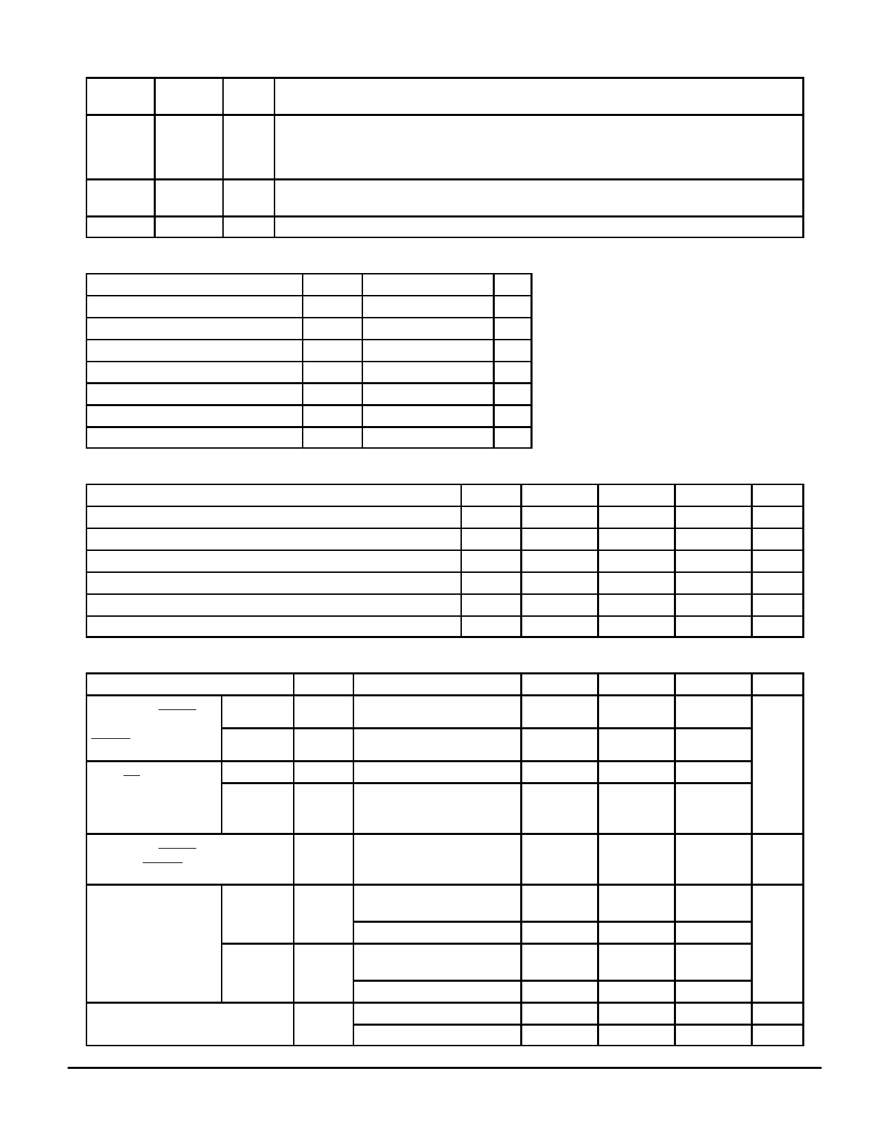
PIN DESCRIPTIONS (continued)
Pin
Location
Symbol
Type
Description
25
TxA2
O Transmit Buffer Output 2 (Inverting) — This pin is the inverting output of the line driver. When VCC =
5 V, + 7 dBm (typ), differential output voltage (VTxA1 – VTxA2), can be obtained with a load of 1.2 kΩ
between pins TxA1 and TxA2. In typical applications, the output level on the telephone line will be half
of the differential output (refer to Application Circuit).
26
TxA1
O Transmit Buffer Output 1 (Non–Inverting) — This pin is the non–inverting output of the line driver.
Refer to TxA2.
27
RxA
I
Receive Signal Input — This pin is the analog signal input which has 500 kΩ input resistance (typ).
ABSOLUTE MAXIMUM RATINGS
Rating
Symbol
Value
Unit
DC Supply Voltage
DC Input Voltage
DC Output Voltage
DC Input Current
DC Output Current
Power Dissipation
Storage Temperature Range
VCC
Vin
Vout
Iin
Iout
PD
Tstg
– 0.5 to + 7.0
V
– 0.5 to VCC + 0.5
V
– 0.5 to VCC + 0.5
V
± 20
mA
± 25
mA
500
mW
– 65 to + 150
°C
This device contains circuitry to protect the
inputs against damage due to high static
voltages or electric fields. However, it is advised
that normal precautions be taken to avoid ap-
plications of any voltage higher than maximum
rated voltages to this high impedance circuit. For
proper operation, it is recommended that Vin and
v Vout be constrained to the range GND (Vin or
v Vout) VCC.
Reliability of operation is enhanced if unused
logic inputs are tied to an appropriate logic volt-
age level (e.g., either GND or VCC).
RECOMMENDED OPERATIONAL CONDITIONS
Parameter
DC Supply Voltage
DC Input Voltage
DC Output Voltage
Crystal Oscillation Frequency
External Input Frequency (ECLK)
Operating Temperature Range
Symbol
Min
VCC
3.3
Vin
0
Vout
0
fosc
—
—
TA
– 30
Typ
5.0
—
—
3.579545
7.15909
25
Max
5.5
VCC
VCC
—
—
+ 85
Unit
V
V
V
MHz
°C
DC ELECTRICAL CHARACTERISTICS (VCC = + 3.3 to + 5.5 V, TA = – 30 to + 85°C)
Characteristic
Symbol
Conditions
Min
Typ
Max
Unit
Input Voltage
High Level
VIH
(TxD, ECLK, RESET,
SCP Rx, SCPCLK,
SCPEN)
Low Level
VIL
0.7 x VCC
—
—
—
—
V
1.1
Output Voltage
(RxD, CD, CLKO,
PB0–3, SCP Tx)
High Level
VOH Vin = VIH or VIL, Iout = 20 µA VCC – 0.1 VCC – 0.01
—
Low Level
VOL
Vin = VIH or VIL
Iout = 20 µA
Iout = 2 mA
—
0.01
0.1
—
—
0.4
Input Leakage Current
(TxD, ECLK, RESET, SCP Rx,
SCPCLK, SCPEN)
Iin
Vin = VCC or GND
—
± 1.0
± 10.0
µA
Quiescent Supply
Current
VCC = 5 V
ICC FSK Mode, RTLA = 0
TxA1 and TxA2 open
—
7
—
mA
DTMF Receive Mode, no input
—
9
—
VCC = 3.6 V ICC FSK Mode, RTLA = 0
TxA1 and TxA2 open
—
6
—
DTMF Receive Mode, no input
—
8
—
Power–Down Supply Current
ICC Power–Down Mode 1
Power–Down Mode 2
—
—
500
µA
—
—
1.0
µA
MC145745
4
MOTOROLA
Share Link: 