NE555 Ver la hoja de datos (PDF) - Philips Electronics
Número de pieza
componentes Descripción
Lista de partido
NE555 Datasheet PDF : 7 Pages
| |||
Philips Semiconductors Linear Products
Timer
Product specification
NE/SA/SE555/SE555C
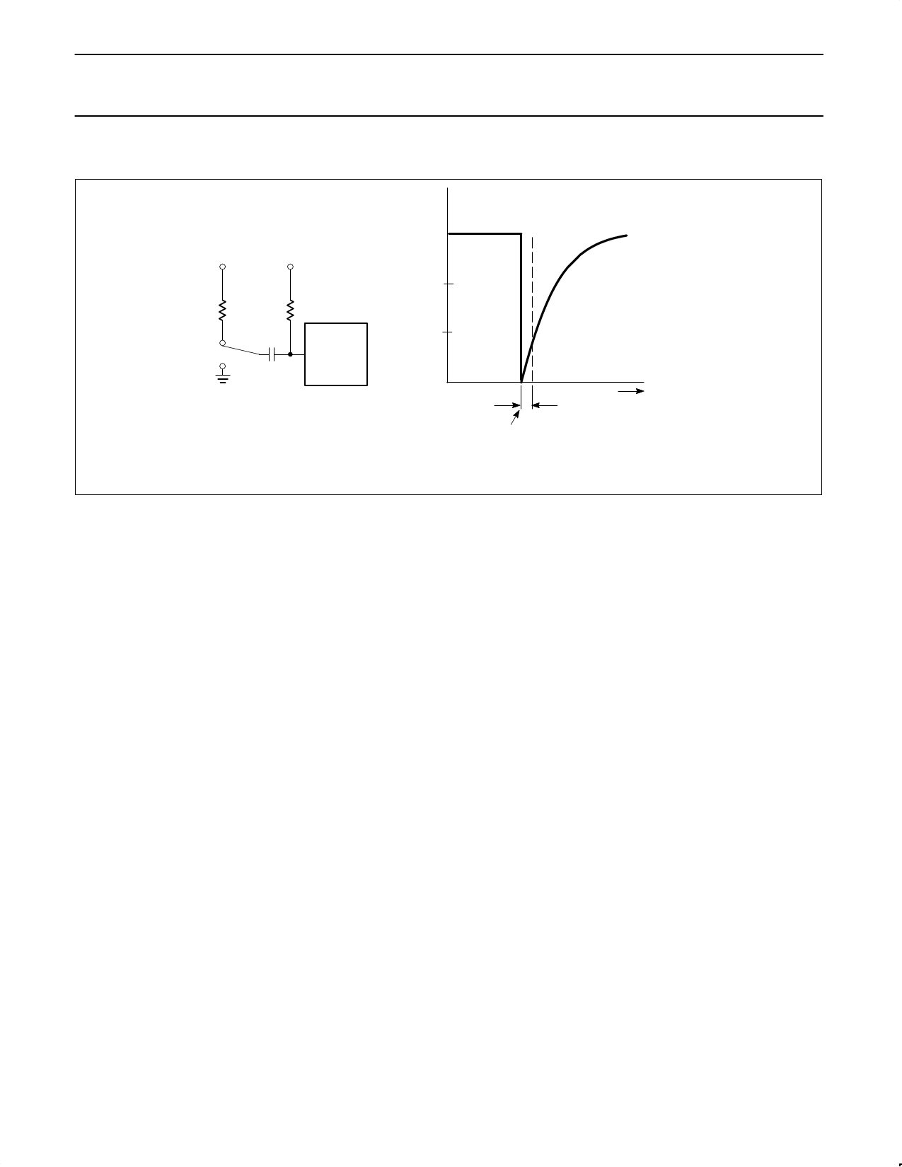
TYPICAL APPLICATIONS
VCC
VCC
VCC
10k
.001µF
2 555
1/3 VCC
OVOLTS
NOTE: All resistor values are in Ω
SWITCH GROUNDED
AT THIS POINT
1
DURATION OF
TRIGGER PULSE AS
SEEN BY THE TIMER
Figure 1. AC Coupling of the Trigger Pulse
Trigger Pulse Width Requirements and Time
Delays
Due to the nature of the trigger circuitry, the timer will trigger on the
negative going edge of the input pulse. For the device to time out
properly, it is necessary that the trigger voltage level be returned to
some voltage greater than one third of the supply before the time out
period. This can be achieved by making either the trigger pulse
sufficiently short or by AC coupling into the trigger. By AC coupling
the trigger, see Figure 1, a short negative going pulse is achieved
when the trigger signal goes to ground. AC coupling is most
frequently used in conjunction with a switch or a signal that goes to
ground which initiates the timing cycle. Should the trigger be held
low, without AC coupling, for a longer duration than the timing cycle
the output will remain in a high state for the duration of the low
trigger signal, without regard to the threshold comparator state. This
is due to the predominance of Q15 on the base of Q16, controlling
the state of the bi-stable flip-flop. When the trigger signal then
returns to a high level, the output will fall immediately. Thus, the
output signal will follow the trigger signal in this case.
Another consideration is the “turn-off time”. This is the measurement
of the amount of time required after the threshold reaches 2/3 VCC
to turn the output low. To explain further, Q1 at the threshold input
turns on after reaching 2/3 VCC, which then turns on Q5, which turns
on Q6. Current from Q6 turns on Q16 which turns Q17 off. This
allows current from Q19 to turn on Q20 and Q24 to given an output
low. These steps cause the 2µs max. delay as stated in the data
sheet.
Also, a delay comparable to the turn-off time is the trigger release
time. When the trigger is low, Q10 is on and turns on Q11 which turns
on Q15. Q15 turns off Q16 and allows Q17 to turn on. This turns off
current to Q20 and Q24, which results in output high. When the
trigger is released, Q10 and Q11 shut off, Q15 turns off, Q16 turns on
and the circuit then follows the same path and time delay explained
as “turn off time”. This trigger release time is very important in
designing the trigger pulse width so as not to interfere with the
output signal as explained previously.
August 31, 1994
352
Share Link: 