TDA9859 Ver la hoja de datos (PDF) - Philips Electronics
Número de pieza
componentes Descripción
Lista de partido
TDA9859 Datasheet PDF : 24 Pages
| |||
Philips Semiconductors
Universal hi-fi audio processor for TV
Product specification
TDA9859
FUNCTIONAL DESCRIPTION
The TDA9859 consists of the following functions:
• Source select switching block
• Loudspeaker channel with effect controls
• Two port outputs for general purpose
• I2C-bus control.
Source select switching block
The TDA9859 selects and switches the input signals from
three stereo or six mono sources MAIN, AUX and SCART
(see Fig.1) to the outputs SCART and loudspeaker
(crossbar-switching; Table 4). The main channel (LINE
outputs) is looped outside the circuit (from pins MOUTR
and MOUTL to pins LINR and LINL), so signals can be
used as LINE output or a surround sound decoder can be
inserted.
Effect controls
‘Linear stereo’, ‘stereo with spatial effect (30% or 52%
anti-phase crosstalk)’ and ‘forced mono with or without
pseudo-stereo effect’ are controlled by three bits. A muting
of 85 dB is provided.
Loudspeaker channel
Volume control is divided into volume control common and
volume control left/right. The common part
(−40 to +15 dB) controls the left and right channels
simultaneously; the left/right part (−23 to 0 dB) controls the
volume of left and right channels independently. Treble
control provides a control range from −12 to +12 dB and
bass control from −12 to +15 dB. Extended bass control
can be provided by an external T-network (see Fig.1) from
−15 to +19 dB (in 2 dB steps).
I2C-bus control
All control settings are stored in subaddress registers.
Data transmission is simplified by auto-incrementing the
subaddresses. The on-chip Power-on reset sets the mute
bit to active, so both the SCART and the loudspeaker
outputs are muted.
The muting can be switched off by writing a ‘0’ (non-muted)
into the mute control bits.
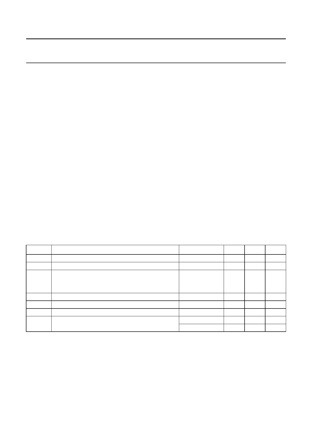
LIMITING VALUES
In accordance with the Absolute Maximum Rating System (IEC 60134).
SYMBOL
PARAMETER
VP
supply voltage (pin VP)
Vn
voltage on all pins, ground excluded
IO
output current
at LOUT and SCOUT pins
at port output pins
Ptot
Tamb
Tstg
Ves
total power dissipation
ambient temperature
storage temperature
electrostatic handling voltage
CONDITIONS
−
−
MIN.
0
0
MAX.
10
VP
UNIT
V
V
−
−
2.5
mA
−
−
1.5
mA
−
−
850 mW
−
0
70
°C
−
−25 +150 °C
all pins; note 1
−
±300 V
all pins; note 2
−
±2000 V
Notes
1. Equivalent to discharging a 200 pF capacitor through a 0 Ω series resistor (machine model).
2. Equivalent to discharging a 100 pF capacitor through a 1.5 kΩ series resistor (human body model).
2001 Jul 11
7
Share Link: 