L4922 Ver la hoja de datos (PDF) - STMicroelectronics
Número de pieza
componentes Descripción
Lista de partido
L4922 Datasheet PDF : 6 Pages
| |||
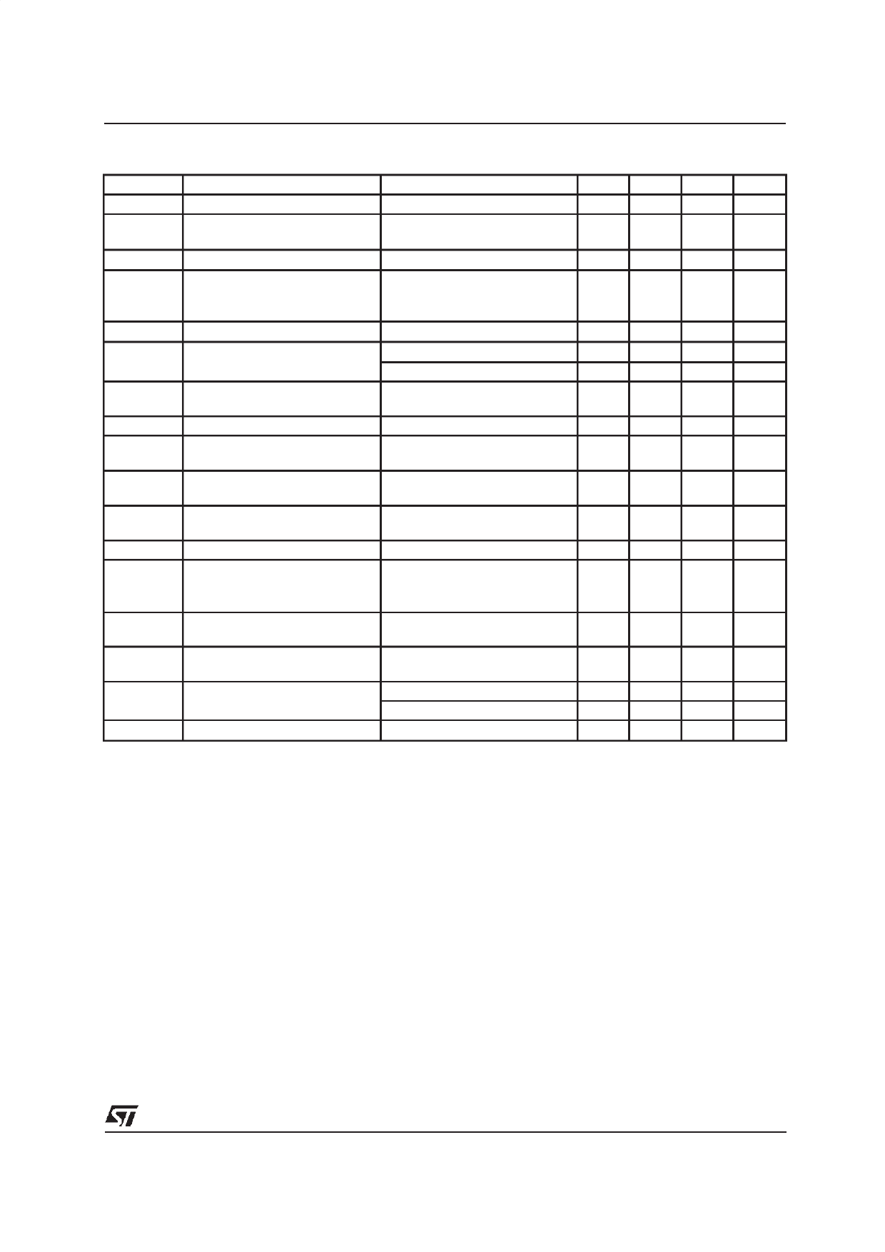
L4922
ELECTRICAL CHARACTERISTICS (Vi = 14. 4V, – 40°C ≤ TJ ≤ + 125°C unless otherwise specified)
Symbol
Vi
Vo
∆VLine
SVR
∆VLOAD
Vi – Vo
Iq
ISC
VR
VRT peak
IR
tD
VRthOFF
IC6
VRthON
V4
V6H
Parameter
Operating Input Voltage
Output Voltage
Line Regulation
Supply Voltage Rejection
Load Regulation
Dropout Voltage
Quiescent Current
Short Circuit Current
Rset Output Saturation Voltage
Power On-Off Reset out Peak
Voltage
Reset Output Leakage Current
(high level)
Reset Pulse Delay Time
Power OFF Vo Threshold
Delay Capacitor Charging
Current (current generator)
Power ON Vo Threshold
Delay Comparator Threshold
Delay Comparator Hysteresis
Test Conditions
(*) Note 1
Io = 0mA to 1A
TJ = 25°C
Vi = 6 to 26V; IO = 10mA
Io = 700mA
f = 120Hz; Co = 47µF
Vi = 12Vdc + 5Vpp
Io = 10mA to 1A
TJ = 25°C, IO = 1A
Over Full T, Io = 1A
Io = 10mA
Io = 1A
1.5V < VO < VRT (off), IR = 1.6mA
3V < VO < VRT (off), IR = 8mA
1KΩ Reset Pull-up to VO
Vo in Regul.
VR = 5V
CD = 100nF
Vo @ Reset out H to L
Transition; TJ = 25°C
– 40°C ≤ TJ ≤ + 125°C
V4 = 3V
Vo @ Reset out L to H
Transition
Reset out = ”1” H to L Transition
Reset out = ”0” L to H Transition
Min.
6
4.8
4.9
Typ.
5
55
Max.
26
5.2
5.1
25
15
50
0.45 0.70
0.90
7
12
25
70
1.8
0.40
0.40
0.65 1.0
50
20
4.75 Vo –0.15
4.70
20
VrthOFF Vo –
+ 0.03V 0.04V
3.2
3.8
3.7
4
4.4
500
Unit
V
V
V
mV
dB
mV
V
V
mA
mA
A
V
V
V
µA
ms
V
V
µA
V
V
V
mV
(*) Note 1 : The device is not operating within the range : 26 V < Vi < 37 V.
EXTERNAL COMPENSATION
Since the purposeof a voltageregulatoris to supply
a fixed output voltage in spite of supply and load
variations, the open loop gain of the regulator must
be very high at low frequencies.This may cause in-
stability as a result of the various poles present in
the loop. To avoid this instability dominant pole
compensationis used to reduce phase shiftsdue to
other poles at the unity gain frequency. The lower
the frequencyof theseother poles, the greater must
be the capacitor used to create the dominant pole
for the same DC gain.
Where the output transistor is a lateral PNP type
there is a pole in the regulation loop at a frequency
too low to be compensated by a capacitor wich can
be integrated. An external compensation is there-
fore necessary so a very high value capacitor must
be connected from the output to ground.
Theparassitic equivalentseries resistanceof theca-
pacitor used adds a zero to the regulation loop. This
zero may compromise the stability of the system
since its effect tends to cancel the effect of the pole
added. In regulatorsthis ESR must be less than 3Ω
and the minimum capacitor value is 47µF.
3/6
Share Link: 