TDA3664 Ver la hoja de datos (PDF) - Philips Electronics
Número de pieza
componentes Descripción
Lista de partido
TDA3664 Datasheet PDF : 16 Pages
| |||
Philips Semiconductors
Very low dropout voltage/quiescent
current 5 V voltage regulator
Preliminary specification
TDA3664
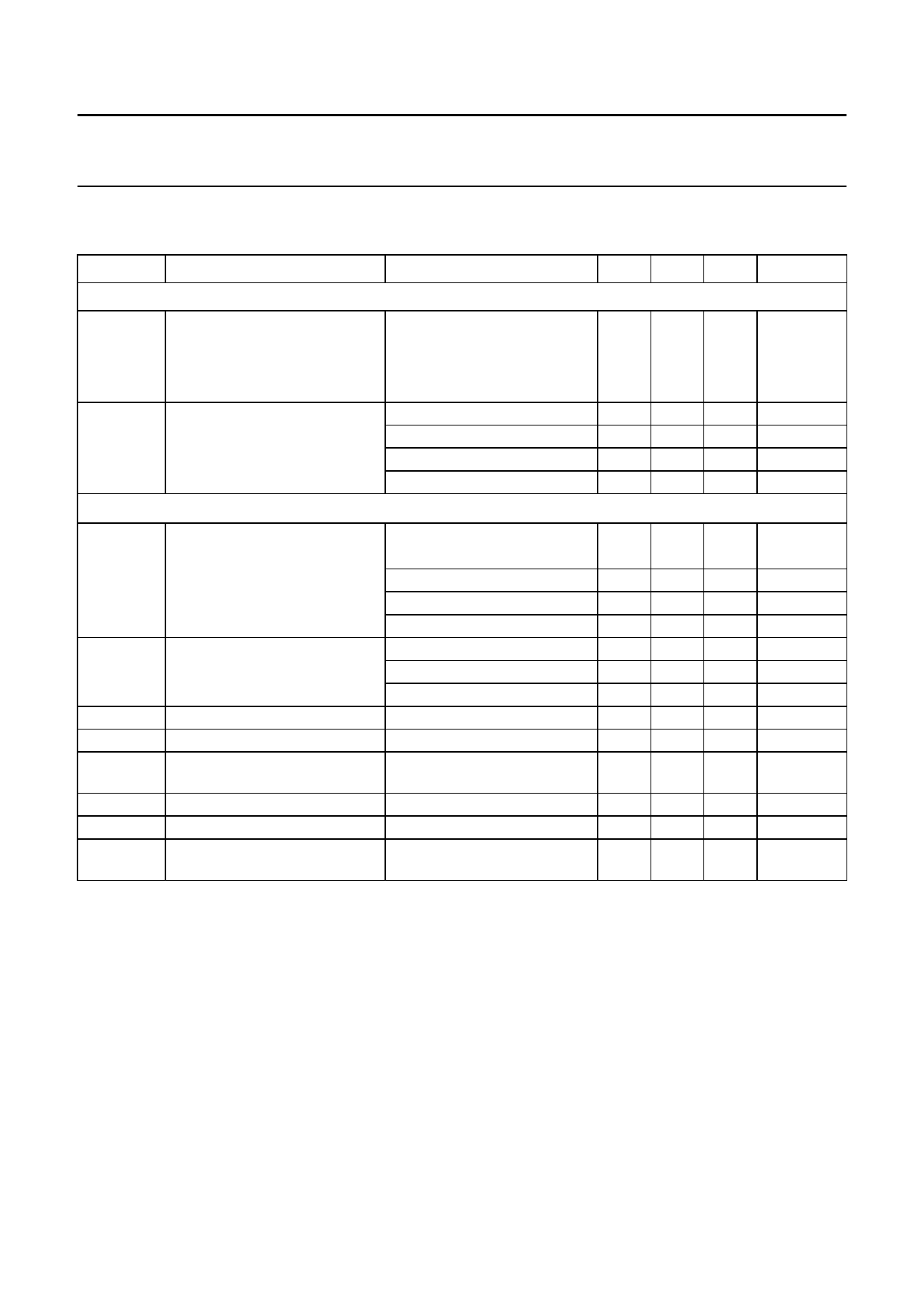
CHARACTERISTICS
VP = 14.4 V; Tamb = 25 °C; see Fig.4; unless otherwise specified.
SYMBOL
PARAMETER
CONDITIONS
MIN. TYP. MAX. UNIT
Supply voltage
VP
supply voltage
TDA3664
regulator operating; note 1
3
TDA3664AT
regulator operating; note 1
3
TDA3664T
regulator operating; note 1
3
Iq
quiescent current
VP = 4.5 V; IREG = 0
−
VP = 14.4 V; IREG = 0
−
6 V ≤ VP ≤ 22 V; IREG = 10 mA −
6 V ≤ VP ≤ 22 V; IREG = 50 mA −
Regulator output: on pin REG (IREG = 0.5 mA), −40 °C ≤ Tamb ≤ 125 °C; note 2
VREG
regulated output voltage
∆VREG(line) line regulation voltage
∆VREG(load)
SVRR
VREG(drop)
load regulation voltage
supply voltage ripple rejection
dropout voltage
IREG(crl)
VREG(stab)
ILO(rp)
current limit
long-term stability
output leakage current
IREG = 0.5 mA,
4.8
8 V ≤ VP ≤ 22 V, Tamb = 25 °C
IREG = 0.5 mA, 8 V ≤ VP ≤ 22 V 4.75
0.5 mA ≤ IREG ≤ 100 mA
4.75
6 V ≤ VP ≤ 45 V; note 2
4.75
8 V ≤ VP ≤ 16 V, Tamb = 25 °C −
7 V ≤ VP ≤ 22 V, Tamb = 25 °C −
7 V ≤ VP ≤ 45 V; note 2
−
0.5 mA ≤ IREG ≤ 50 mA
−
fi = 120 Hz; Vripple = 1 Vrms
50
IREG = 50 mA; VP = 4.5 V;
−
Tamb ≤ 85 °C
VREG > 4.5 V
0.17
−
with reverse polarity input
−
VP = −15 V, VREG ≤ 0.3 V
14.4
14.4
14.4
10
15
0.2
1.4
5.0
5.0
5.0
5.0
1
1
1
10
60
0.18
0.25
20
1
45
45
33
−
30
0.5
2.5
5.2
5.25
5.25
5.25
10
30
50
50
−
0.3
−
−
500
V
V
V
µA
µA
mA
mA
V
V
V
V
mV
mV
mV
mV
dB
V
A
mV/1000 h
µA
Notes
1. The regulator output will follow VP if VP < VREG + VREG(drop)
2. TDA3664T: VP ≤ 22 V; −40 °C ≤ Tamb ≤ 85 °C.
1999 Sep 01
5
Share Link: 