RF2485 Ver la hoja de datos (PDF) - RF Micro Devices
Número de pieza
componentes Descripción
Lista de partido
RF2485 Datasheet PDF : 8 Pages
| |||
Preliminary
RF2485
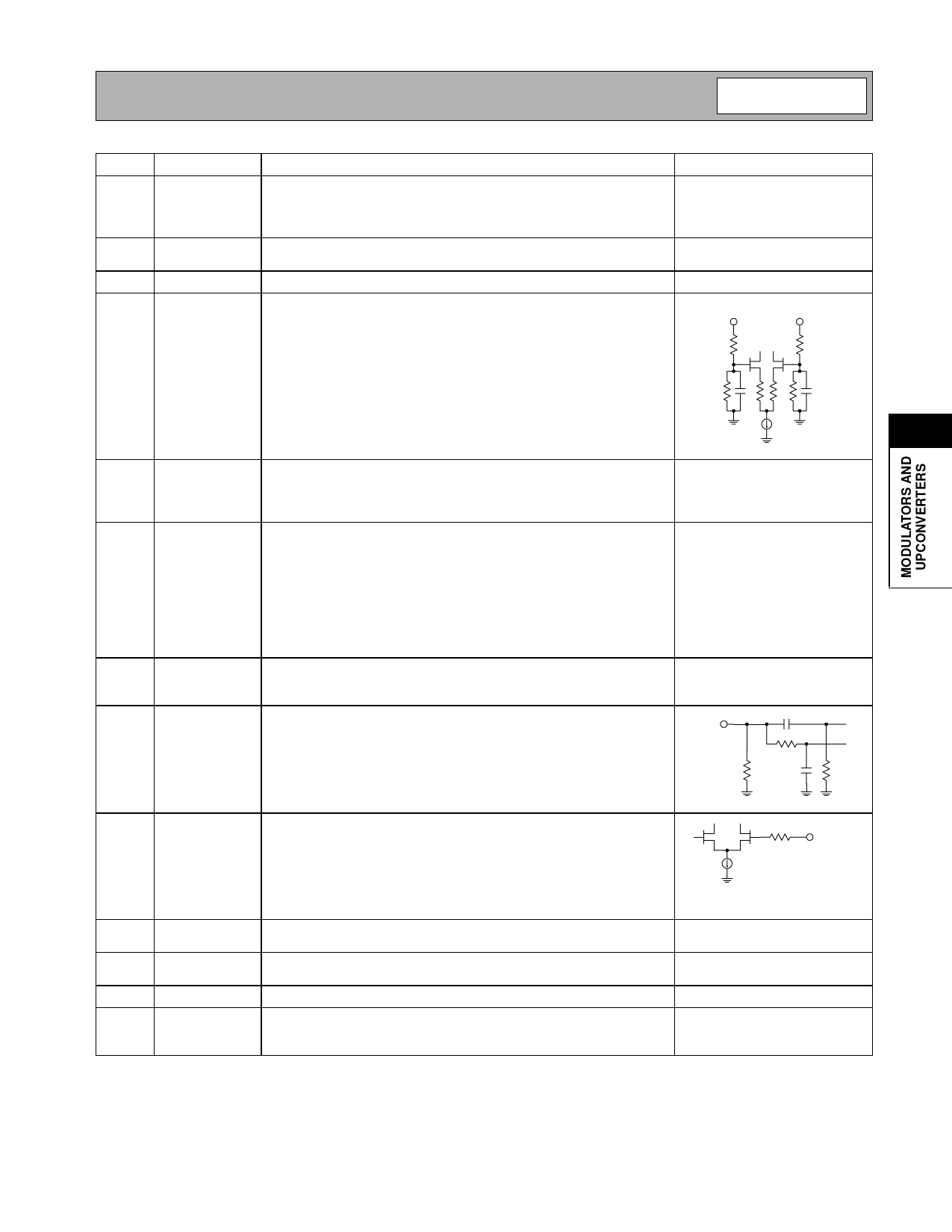
Pin Function Description
Interface Schematic
1
VDD2
Power supply for the RF Output amplifier. An external RF bypass
capacitor is needed. The trace length between the pin and the bypass
capacitor should be minimized. The ground side of the capacitor should
connect immediately to the ground plane.
2
VDD1
Power supply for all other circuits. An external RF bypass capacitor is
needed.
3
NC
No connection.
4
I SIG
Baseband input to the I mixer. This pin is DC coupled. Maximum output
I REF
I SIG
power is obtained when the input signal has a peak to peak amplitude
of 5V. The DC level supplied to this pin should be 2.5±0.5V. The SIG
and REF inputs are inputs of a differential amplifier. Therefore the REF
and SIG inputs are interchangeable. If swapping the I SIG and I REF
pins, the Q SIG and Q REF also need to be swapped to maintain the
correct phase. It is also possible to drive the SIG and REF inputs in a
balanced mode. This will increase the gain.
5
5
I REF
Reference voltage for the I mixer. This voltage should be the same as See pin 4.
the DC voltage supplied to the I SIG pin. To obtain a carrier suppres-
sion of better than 40dB it may be tuned ±0.15V (relative to the I SIG
DC voltage). Without tuning, it will typically be better than 25dB.
6
Q REF
Reference voltage for the Q mixer. This voltage should be the same as Same as pin 3.
the DC voltage supplied to the Q SIG pin. To obtain a carrier suppres-
sion of better than 40dB it may be tuned ±0.15V (relative to the Q SIG
DC voltage). Without tuning, it will typically be better than 25dB. The
SIG and REF inputs are inputs of a differential amplifier. Therefore the
REF and SIG inputs are interchangeable. If swapping the I SIG and I
REF pins, Q SIG and Q REF also need to be swapped to maintain cor-
rect phase. It is also possible to drive the SIG and REF inputs in a bal-
anced mode. This will increase the gain.
7
Q SIG
Baseband input to the Q mixer. This pin is DC coupled. Maximum out- Same as pin 4.
put power is obtained when the input signal has a peak to peak ampli-
tude of 5V. The DC level supplied to this pin should be 2.5±0.5V.
8
LO IN
The input of the phase shifting network. This high impedance input can
be matched with an external 56Ω termination resistor. This pin is inter-
LO IN
nally connected to ground through a 4kΩ resistor. Putting a DC voltage
on this pin is not recommended. However, connecting this pin to
ground, e.g., through a shunt inductor, is allowed.
9
PHASE This pin allows to adjust the phase of the I/Q signals. However, the con-
trol is very sensitive and hard to control. Control voltage change for a
few degrees adjustment is in the order of 10mV. Device to device and
temperature variation are not characterized. Therefore it is not recom-
mended to use this pin; leave it not connected. Do NOT connect to
ground.For compensating large errors in the I/Q signals supplied to the
device or in control loops this pin may prove useful.
10
GND1
Ground connection of the LO phase shift network. This pin should be
connected directly to the ground plane.
11
GND
Ground connection for other circuits. Keep traces short and connect to
ground plane immediately.
12
GND
Same as pin 11.
13
GND2
Ground connection for the RF output stage. A good ground connection
is especially important at this pin to avoid interference with other cir-
cuits.
PHASE
Rev A3 010820
5-57
Share Link: 