RF2469 Ver la hoja de datos (PDF) - RF Micro Devices
Número de pieza
componentes Descripción
Lista de partido
RF2469 Datasheet PDF : 18 Pages
| |||
Preliminary
8
Typical Applications
• W-CDMA Handsets
• PCS Handsets
• General Purpose Downconverter
RF2469
W-CDMA AND PCS LOW NOISE
AMPLIFIER/MIXER DOWNCONVERTER
• Commercial and Consumer Systems
• Portable Battery-Powered Equipment
Product Description
1.00
0.90
4.00
sq.
The RF2469 is a receiver front-end designed for the
0.60
receive section of W-CDMA and PCS applications. It is
0.24 typ
0.65
0.30
4 PLCS
designed to amplify and downconvert RF signals while
providing 23dB of stepped gain control range and fea-
3 0.20
2.10
sq.
tures digital control of the LNA gain and mixer gain. A fur-
ther feature of the chip is adjustable IIP3 of the LNA and
mixer using an off-chip current setting resistor. Noise Fig-
12°
0.75
ure, IP3, and other specs are designed to be compatible
MAX
0.50
0.23
with W-CDMA and PCS communications. The IC is man-
0.05
0.50
0.13
4 PLCS
ufactured on an advanced Gallium Arsenide Heterojunc-
Dimensions in mm.
NOTES:
Note orientation of package.
8
tion Bipolar Transistor (GaAs HBT) process and
packaged in a 20-pin, leadless chip carrier with an
exposed die flag.
1 Shaded lead is Pin 1.
2 Pin 1 identifier must exist on top surface of package by identification
mark or feature on the package body. Exact shape and size is optional.
3 Dimension applies to plated terminal: to be measured between 0.02 mm
and 0.25 mm from terminal end.
4 Package Warpage: 0.05 mm max.
5 Die Thickness Allowable: 0.305 mm max.
Optimum Technology Matching® Applied
Si BJT
üGaAs HBT
GaAs MESFET
Si Bi-CMOS
SiGe HBT
Si CMOS
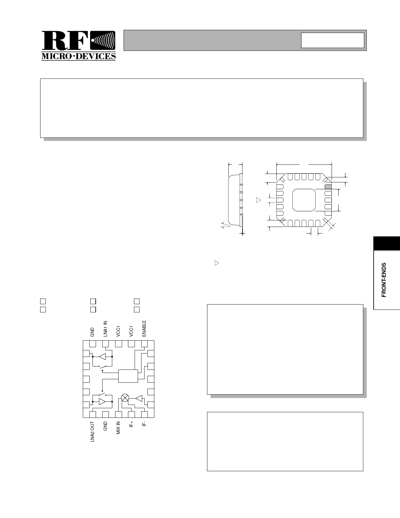
20 19 18 17 16
LNA1 OUT 1
15 LNA1 BYP
GND 2
VCC1 3
Logic
Control
14
LNA2
BYP
13 GND
VCC1 4
12 VCC1
LNA2 IN 5
11 LO IN
6 7 8 9 10
Functional Block Diagram
Package Style: LCC, 20-Pin, 4x4
Features
• Complete Receiver Front-End
• Stepped LNA/Mixer Gain Control
• Adjustable LNA/Mixer Bias Current
• 23dB Maximum Cascade Gain
• 2.5dB Noise Figure at Maximum
Cascade Gain
Ordering Information
RF2469
RF2469 PCBA
W-CDMA and PCS Low Noise Amplifier/Mixer Down-
converter
Fully Assembled Evaluation Board
RF Micro Devices, Inc.
7628 Thorndike Road
Greensboro, NC 27409, USA
Tel (336) 664 1233
Fax (336) 664 0454
http://www.rfmd.com
Rev A5 010717
8-33
Share Link: 