LPC47B37X Ver la hoja de datos (PDF) - SMSC -> Microchip
Número de pieza
componentes Descripción
Lista de partido
LPC47B37X
SMSC -> Microchip

LPC47B37X Datasheet PDF : 254 Pages
| |||
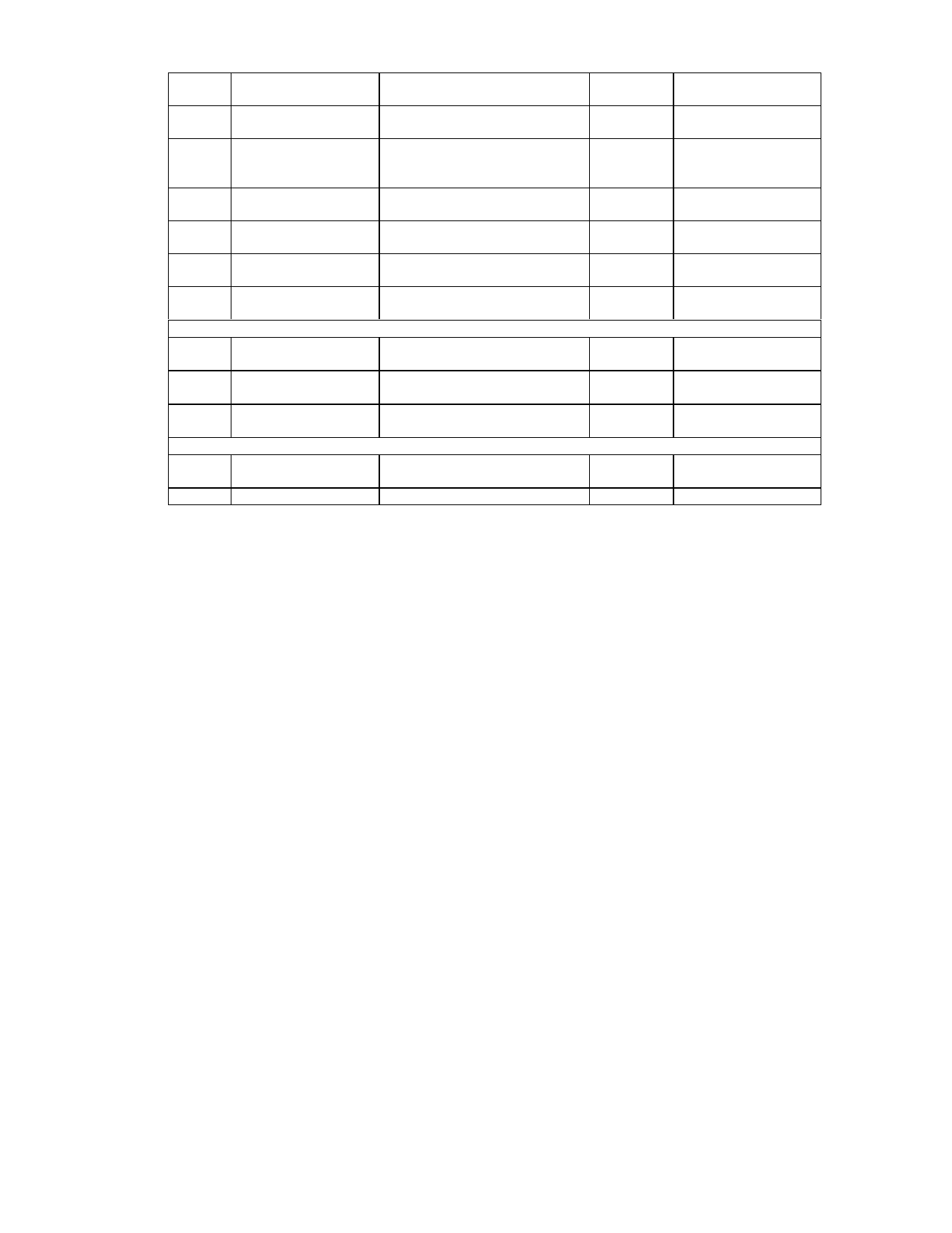
PIN #
NAME
95
GP52 /RXD2/IRRX
96
GP53 /TXD2/IRTX
97
GP54 /nDSR2
98
GP55/nRTS2
99
GP56/nCTS2
100
GP57/nDTR2
53, 65, VCC
93
18
VTR
7, 31, VSS
60, 76
6
CLKI32
19
CLOCKI
FUNCTION
General Purpose I/O /Receive
Data 2/IRRX
General Purpose I/O /Transmit
Data 2/IRTX
(Note 5)
General Purpose I/O /Data Set
Ready 2
General Purpose I/O /Request
to Send 2
General Purpose I/O /Clear to
Send 2
General Purpose I/O /Data
Terminal Ready 2
POWER PINS
+3.3 Volt Supply Voltage
BUFFER
TYPE
IS/O8
IO12
IO8
IO8
IO8
IO8
BUFFER TYPE PER
FUNCTION (NOTE 1)
(IS/O8/OD8)/IS/IS
(I/O12/OD12)/O12/O
12
(I/O8/OD8)/I
(I/O8/OD8)/O8
(I/O8/OD8)/I
(I/O8/OD8)/O8
+3.3 Volt Standby Supply
Voltage (Note 6)
Ground
CLOCK PINS
32.768kHz Standby Clock
IS
IS
Input (Note 3)
14.318MHz Clock Input
IS
IS
Note: The "n" as the first letter of a signal name indicates an "Active Low" signal.
Note 1: Buffer types per function on multiplexed pins are separated by a slash “/”. Buffer types in
parenthesis represent multiple buffer types for a single pin function.
Note 2: The nLPCPD pin may be tied high. The LPC interface will function properly if the
nPCI_RESET signal follows the protocol defined for the nLRESET signal in the “Low Pin Count
Interface Specification”.
Note 3: If the 32kHz input clock is not used the CLKI32 pin must be grounded. There is a bit in the
configuration register at 0xF0 in Logical Device A that indicates whether or not the 32KHz
clock is connected. This bit determines the clock source for the fan tachometer, LED and
“wake on specific key” logic. Set this bit to ‘1’ if the clock is not connected.
Note 4: The fan control pin (FAN) comes up as output and low following a VCC POR and Hard Reset.
This pin reverts to its non-inverting General Purpose I/O output function when VCC is removed
from the part.
Note 5: The GP53/TXD2/IRTX pin is an output and low when the part is under VTR power (VCC=0).
The pin comes up as output and low following a VCC POR and Hard Reset.
Note 6: VTR can be connected to VCC if no wakeup functionality is required.
Note 7: The GP24/SYSOPT pin requires an external pulldown resistor to put the base I/O address for
configuration at 0x02E. An external pullup resistor is required to move the base I/O address
for configuration to 0x04E.
9
Share Link: