FDC37C67X Ver la hoja de datos (PDF) - SMSC -> Microchip
Número de pieza
componentes Descripción
Lista de partido
FDC37C67X Datasheet PDF : 194 Pages
| |||
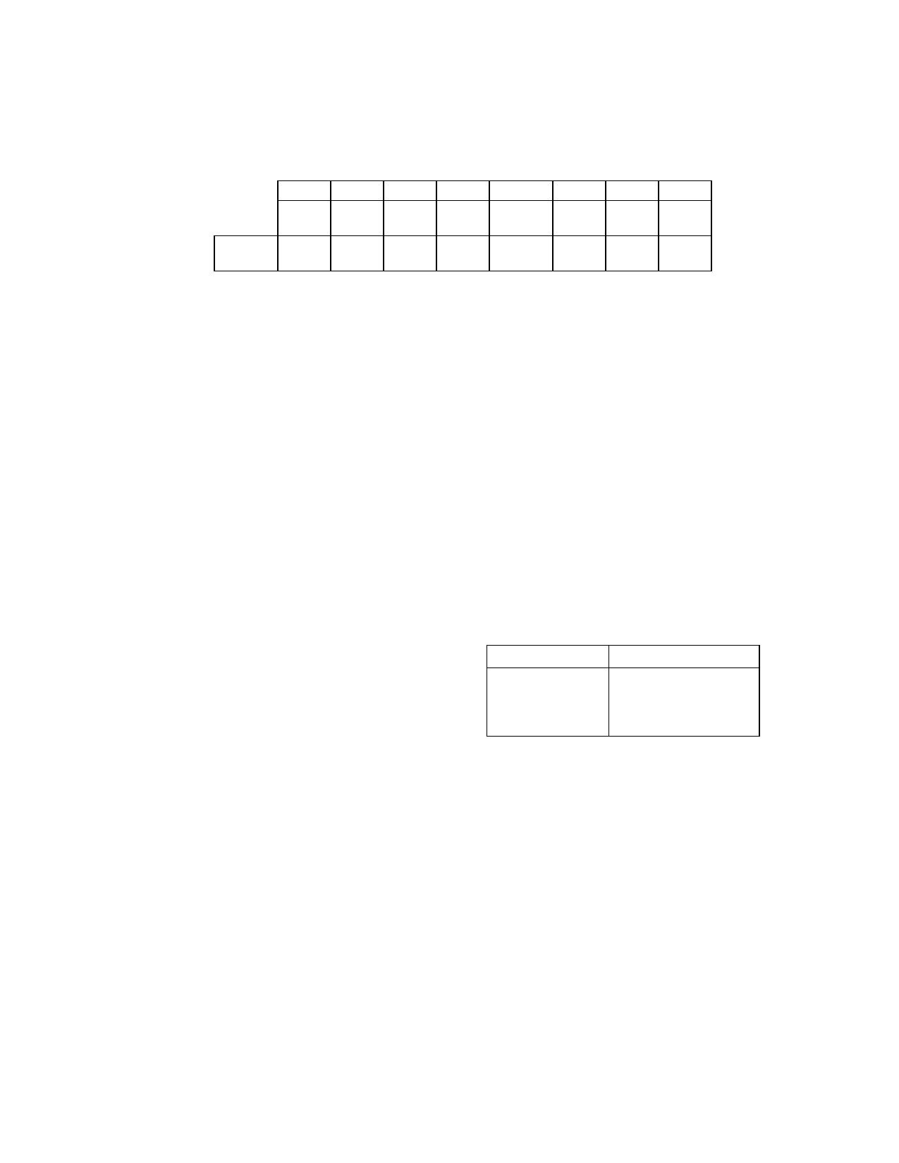
DIGITAL OUTPUT REGISTER (DOR)
Address 3F2 READ/WRITE
The DOR controls the drive select and motor
enables of the disk interface outputs. It
also contains the enable for the DMA logic and a
software reset bit. The contents of the DOR are
unaffected by a software reset. The DOR can
be written to at any time.
RESET
COND.
7
MOT
EN3
0
6
MOT
EN2
0
5
MOT
EN1
0
4
MOT
EN0
0
3
2
DMAEN nRESE
T
0
0
1
DRIVE
SEL1
0
0
DRIVE
SEL0
0
BIT 0 and 1 DRIVE SELECT
These two bits are binary encoded for the four
drive selects DS0 -DS3, thereby allowing only
one drive to be selected at one time.
BIT 2 nRESET
A logic "0" written to this bit resets the Floppy
disk controller. This reset will remain active
until a logic "1" is written to this bit. This
software reset does not affect the DSR and CCR
registers, nor does it affect the other bits of the
DOR register. The minimum reset duration
required is 100ns, therefore toggling this bit by
consecutive writes to this register is a valid
method of issuing a software reset.
BIT 3 DMAEN
PC/AT and Model 30 Mode:
Writing this bit to logic "1" will enable the DRQ,
nDACK, TC and FINTR outputs. This bit being
a logic "0" will disable the nDACK and TC
inputs, and hold the DRQ and FINTR outputs in
a high impedance state. This bit is a logic "0"
after a reset and in these modes.
PS/2 Mode: In this mode the DRQ, nDACK, TC
and FINTR pins are always enabled. During a
reset, the DRQ, nDACK, TC, and FINTR pins
will remain enabled, but this bit will be cleared to
a logic "0".
BIT 4 MOTOR ENABLE 0
This bit controls the MTR0 disk interface output.
A logic "1" in this bit will cause the output pin to
go active.
BIT 5 MOTOR ENABLE 1
This bit controls the MTR1 disk interface output.
A logic "1" in this bit will cause the output pin to
go active.
BIT 6 MOTOR ENABLE 2
This bit controls the MTR2 disk interface output.
A logic "1" in this bit will cause the output pin to
go active.
BIT 7 MOTOR ENABLE 3
This bit controls the MTR3 disk interface output.
A logic "1" in this bit causes the output to go
active.
Table 3 - Drive Activation Values
DRIVE
0
1
2
3
DOR VALUE
1CH
2DH
4EH
8FH
18
Share Link: 