COM81C17LJP Ver la hoja de datos (PDF) - SMSC -> Microchip
Número de pieza
componentes Descripción
Lista de partido
COM81C17LJP Datasheet PDF : 18 Pages
| |||
INTERRUPT MASK REGISTER DESCRIPTION REGISTER DECODE & TRUTH TABLE
This is an eight bit write only register which is
loaded by the processor. These bits are used to
enable interrupts from the corresponding bits in
the Status Register. This register is reset with
internal reset.
The TPUART provides unique decode capability
to three of the seven internal processor
accessible register. These are the RX Buffer
Register (read only), the Status Register (read
only) and the Control Register (write only). The
other four registers (write only) are decoded in a
sequential manner following reset. Refer to
table below:
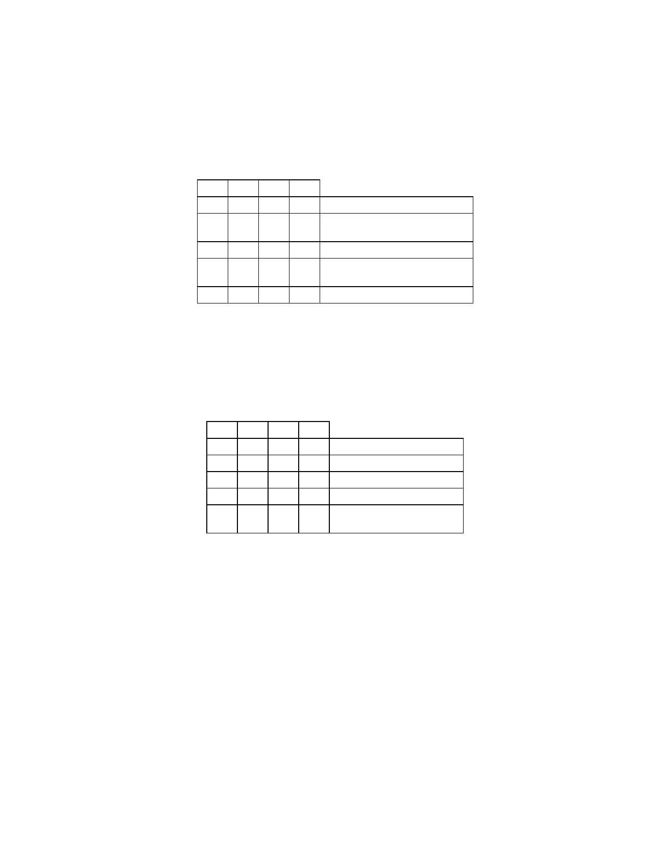
Table 6 - DECODE TRUTH TABLE
RS nRD nWR nCS
0
0
1
0 READ RX BUFFER REGISTER
0
1
0
0 WRITE TO TX BUFFER
REGISTER
1
0
1
0 READ STATUS REGISTER
1
1
0
0 WRITE TO CONTROL
REGISTER
X X X 1 DATA BUS IN TRI STATE
The first write to address zero (RS = 0) will
access the Mode Register, the second will
access the Interrupt Mask Register, the third will
access the Baud Rate Select Register, the fourth
and all subsequent writes will access the TX
Buffer Register.
Following reset, the decode sequence of writes
to address 0 is as follows:
RS0 - Selects the Mode Control Register
RS1 - Selects the Interrupt Mask Register
RS2 - Selects the Baud Rate Select Register
RS3 - Selects the TX Buffer Register
Table 7 - INTERNAL REGISTER SELECT
RS0 RS1 RS2 RS3
0
1
1
1 AFTER RESET
1
0
1
1 AFTER FIRST WRITE
1
1
0
1 AFTER SECOND WRITE
1
1
1
0 AFTER THIRD WRITE
1
1
1
0 ALL SUBSEQUENT
WRITES
11
Share Link: 