74ABT16821A Ver la hoja de datos (PDF) - Philips Electronics
Número de pieza
componentes Descripción
Lista de partido
74ABT16821A
Philips Electronics

74ABT16821A Datasheet PDF : 10 Pages
| |||
Philips Semiconductors
20-bit bus-interface D-type flip-flop;
positive-edge trigger (3-State)
Product specification
74ABT16821A
74ABTH16821A
AC CHARACTERISTICS
GND = 0V, tR = tF = 2.5ns, CL = 50pF, RL = 500Ω
SYMBOL
PARAMETER
WAVEFORM
fMAX
Maximum clock frequency
1
tPLH
Propagation delay
tPHL
nCP to nQx
1
tPZH
Output enable time
3
tPZL
to High and Low level
4
tPHZ
Output disable time
3
tPLZ
from High and Low level
4
AC SETUP REQUIREMENTS
GND = 0V, tR = tF = 2.5ns, CL = 50pF, RL = 500Ω
SYMBOL
PARAMETER
WAVEFORM
ts(H)
ts(L)
Setup time, High or Low
nDx to nCP
2
th(H)
th(L)
Hold time, High or Low
nDx to nCP
2
tw(H)
tw(L)
nCP pulse width
High or Low
1
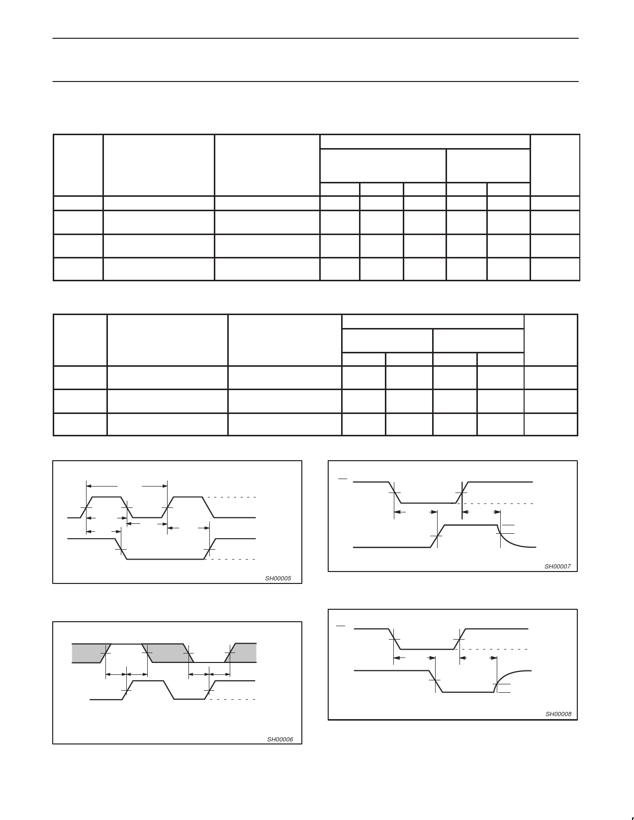
AC WAVEFORMS
1/fMAX
nCP
VM
tw(H)
tPHL
VM
tw(L)
VM
tPLH
nQx
VM
VM
3.0V or VCC
whichever
is less
0V
VOH
VOL
SH00005
Waveform 1. Propagation Delay, Clock Input to Output,
Clock Pulse Width, and Maximum Clock frequency
nDx
CP
VM VM
ts(H) th(H)
VM
VM VM
ts(L) th(L)
VM
3.0V or VCC
whichever
is less
0V
3.0V or VCC
whichever
is less
0V
SH00006
Waveform 2. Data Setup and Hold Times
LIMITS
Tamb = +25oC
VCC = +5.0V
MIN
TYP
MAX
160
250
1.3
2.4
3.3
1.1
2.0
2.6
1.4
2.5
3.3
1.2
2.3
3.0
1.6
3.2
4.1
1.3
2.3
3.1
Tamb = -40 to
+85oC
VCC = +5.0V ±0.5V
MIN
MAX
160
1.3
3.7
1.1
3.0
1.4
4.1
1.2
3.7
1.6
4.8
1.3
3.3
UNIT
MHz
ns
ns
ns
LIMITS
Tamb = +25oC
VCC = +5.0V
MIN
TYP
Tamb = -40 to +85oC
VCC = +5.0V ±0.5V
MIN
MAX
1.8
1.2
1.8
1.8
–0.9
1.8
1.0
0.8
1.0
1.0
–1.0
1.0
2.5
0.8
2.5
2.5
1.0
2.5
UNIT
ns
ns
ns
nOE
nQx
VM
tPZH
VM
tPHZ
VM
3.0V or VCC
whichever
is less
0V
VOH
VY
0V
SH00007
Waveform 3. 3-State Output Enable Time to High Level
and Output Disable Time from High Level
nOE
nQx
VM
tPZL
VM
tPLZ
VM
3.0V or VCC
whichever
is less
0V
VX
VOL
3.0V or VCC
0V
SH00008
Waveform 4. 3-State Output Enable Time to Low Level
and Output Disable Time from Low Level
1998 Feb 27
6
Share Link: