74LVX541M Ver la hoja de datos (PDF) - Fairchild Semiconductor
Número de pieza
componentes Descripción
Lista de partido
74LVX541M Datasheet PDF : 6 Pages
| |||
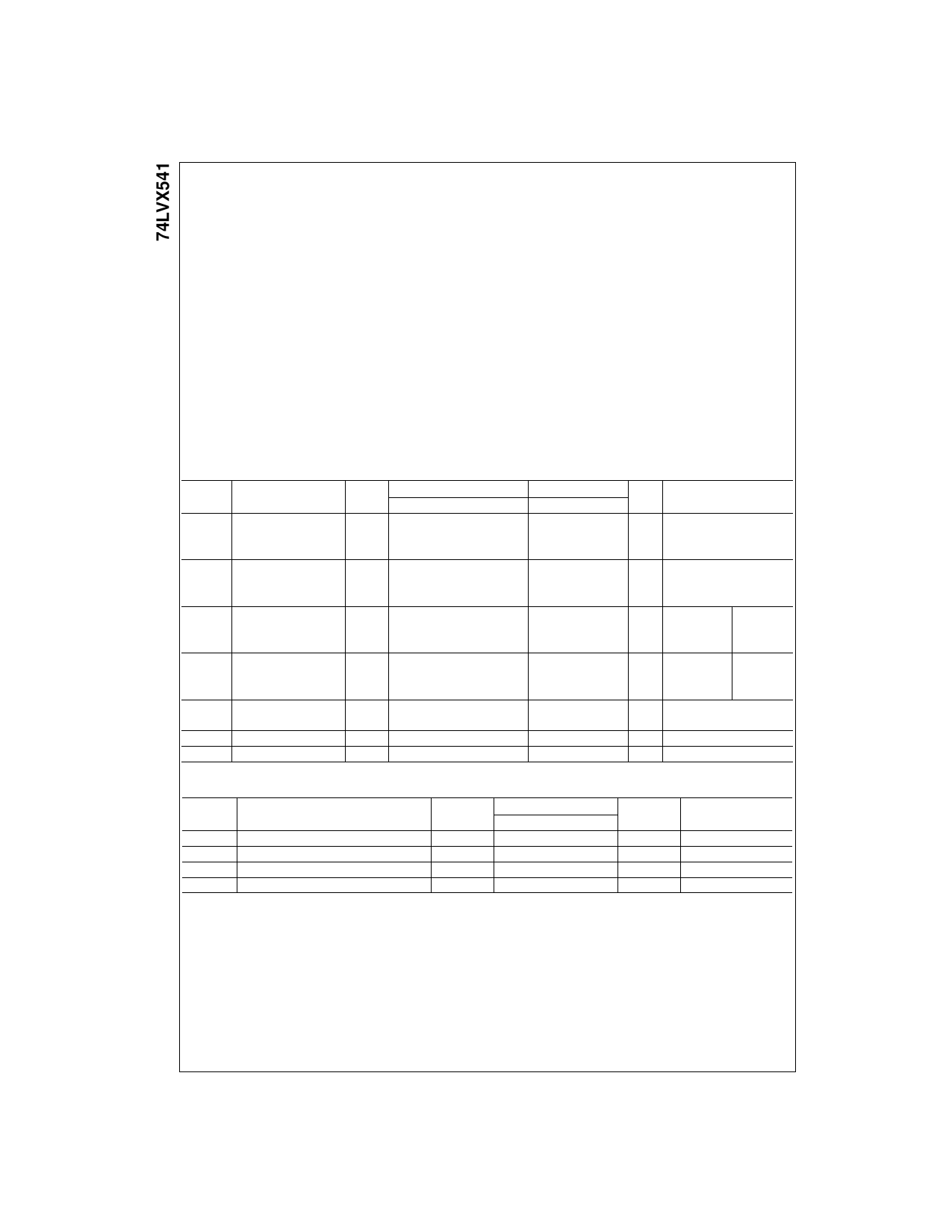
Absolute Maximum Ratings(Note 1)
Supply Voltage (VCC)
DC Input Diode Current (IIK)
VI 0.5V
DC Input Voltage (VI)
DC Output Diode Current (IOK)
VO 0.5V
VO VCC 0.5V
DC Output Voltage (VO)
DC Output Source
or Sink Current (IO)
DC VCC or Ground Current
(ICC or IGND)
Storage Temperature (TSTG)
Power Dissipation
0.5V to 7.0V
20 mA
0.5V to 7V
20 mA
20 mA
0.5V to VCC 0.5V
r25 mA
r75 mA
65qC to 150qC
180 mW
Recommended Operating
Conditions (Note 2)
Supply Voltage (VCC)
Input Voltage (VI)
Output Voltage (VO)
Operating Temperature (TA)
Input Rise and Fall Time ('t/'V)
2.0V to 3.6V
0V to 5.5V
0V to VCC
40qC to 85qC
0 ns/V to 100 ns/V
Note 1: The “Absolute Maximum Ratings” are those values beyond which
the safety of the device cannot be guaranteed. The device should not be
operated at these limits. The parametric values defined in the Electrical
Characteristics tables are not guaranteed at the absolute maximum ratings.
The “Recommended Operating Conditions” table will define the conditions
for actual device operation.
Note 2: Unused inputs must be held HIGH or LOW. They may not float
DC Electrical Characteristics
Symbol
Parameter
VCC
VIH
HIGH Level Input
2.0
Voltage
3.0
3.6
VIL
LOW Level Input
2.0
Voltage
3.0
3.6
VOH
HIGH Level Output
2.0
Voltage
3.0
3.0
VOL
LOW Level Output
2.0
Voltage
3.0
3.0
IOZ
3-STATE Output
3.6
OFF-State Current
IIN
Input Leakage Current
3.6
ICC
Quiescent Supply Current 3.6
TA 25qC
Min
Typ
Max
TA 40qC to 85qC
Units
Min
Max
Conditions
1.5
1.5
2.0
2.0
V
2.4
2.4
0.5
0.5
0.8
0.8
V
0.8
0.8
1.9
2.9
2.58
2.0
1.9
3.0
2.9
2.48
0.0
0.1
0.0
0.1
0.36
r0.25
r0.1
4.0
0.1
0.1
0.44
r2.5
r1.0
40.0
IOH 50 PA
V VIN VIH or VIL IOH 50 PA
IOH 4 mA
IOL 50 PA
V VIN VIH or VIL IOL 50 PA
IOL 4 mA
PA VIN VIH or VIL
VOUT VCC or GND
PA VIN 5.5V or GND
PA VIN VCC or GND
Noise Characteristics (Note 3)
Symbol
Parameter
VCC
(V)
VOLP
Quiet Output Maximum Dynamic VOL
3.3
VOLV
Quiet Output Minimum Dynamic VOL
3.3
VIHD
Minimum HIGH Level Dynamic Input Voltage
3.3
VILD
Maximum HIGH Level Dynamic Input Voltage
3.3
Note 3: Input tr tf 3 ns.
TA 25qC
Typ
Limits
0.5
0.8
0.5
0.8
2.0
0.8
Units
V
V
V
V
Conditions
CL 50 pF
CL 50 pF
CL 50 pF
CL 50 pF
www.fairchildsemi.com
2
Share Link: 