A418316 Ver la hoja de datos (PDF) - AMIC Technology
Número de pieza
componentes Descripción
Lista de partido
A418316 Datasheet PDF : 25 Pages
| |||
Selection Guide
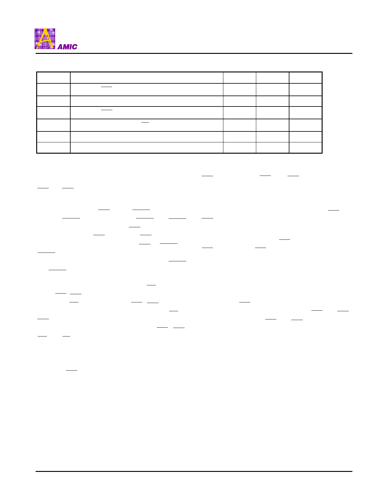
Symbol
tRAC
tAA
tCAC
tOEA
tRC
tPC
Description
Maximum RAS Access Time
Maximum Column Address Access Time
Maximum CAS Access Time
Maximum Output Enable ( OE ) Access Time
Minimum Read or Write Cycle Time
Minimum FAST Cycle Time
Functional Description
The A418316 reads and writes data by multiplexing an 18-
bit address into a 9-bit row and 9-bit column address.
RAS and CAS are used to strobe the row address and the
column address, respectively.
The A418316 has two CAS inputs: LCAS controls I/O0-
I/O7, and UCAS controls I/O8 - I/O15, UCAS and LCAS
function in an identical manner to CAS in that either will
generate an internal CAS signal. The CAS function and
timing are determined by the first CAS ( UCAS or
LCAS ) to transition low and by the last to transition high.
Byte Read and Byte Write are controlled by using LCAS
and UCAS separately.
A Read cycle is performed by holding the WE signal high
during RAS / CAS operation. A Write cycle is executed by
holding the WE signal low during RAS / CAS operation;
the input data is latched by the falling edge of WE or
CAS , whichever occurs later. The data inputs and outputs
are routed through 16 common I/O pins, with RAS , CAS ,
WE and OE controlling the in direction.
FAST Page Mode operation all 512 columns within a
selected row to be randomly accessed at a high data rate.
A FAST Page Mode cycle is initiated with a row address
latched by RAS followed by a column address latched by
A418316 Series
-25
-35
Unit
25
35
ns
12
17
ns
8
10
ns
8
10
ns
44
62
ns
15
19
ns
CAS . While holding RAS low, CAS can be toggled to
strobe changing column addresses, thus achieving shorter
cycle times.
The A418316 offers an accelerated Fast Page Mode cycle.
A memory cycle is terminated by returning both RAS and
CAS high. Memory cell data will retain its correct state by
maintaining power and accessing all 512 combinations of
the 9-bit row addresses, regardless of sequence, at least
once every 8ms through any RAS cycle (Read, Write) or
RAS Refresh cycle ( RAS -only, CBR, or Hidden). The CBR
Refresh cycle automatically controls the row addresses by
invoking the refresh counter and controller.
Power-On
The initial application of the VCC supply requires a 200 µs
wait followed by a minimum of any eight initialization cycles
containing a RAS clock. During Power-On, the VCC
current is dependent on the input levels of RAS and CAS .
It is recommended that RAS and CAS track with VCC or
be held at a valid VIH during Power-On to avoid current
surges.
PRELIMINARY (July, 2003,Version 0.0)
2
AMIC Technology, Inc.
Share Link: 