RT9181 Ver la hoja de datos (PDF) - Richtek Technology
Número de pieza
componentes Descripción
Lista de partido
RT9181 Datasheet PDF : 10 Pages
| |||
Preliminary
RT9181
power dissipation across the device is
P = IOUT (VIN – VOUT)
The GND pin of the RT9181 performs the dual
function of providing an electrical connection to
ground and channeling heat away, Connect the GND
pin to ground using a large pad or ground plane.
Capacitor Selection and Regulator Stability
Like any low-dropout regulator, the external
capacitors used with the RT9181 must be carefully
selected for regulator stability and performance.
Using a capacitor whose value is ≥ 1µF on the
RT9181 input and the amount of capacitance can be
increased without limit. The input capacitor must be
located a distance of not more than 0.5” from the
input pin of the IC and returned to a clean analog
ground. Any good quality ceramic or tantalum can be
used for this capacitor. The capacitor with larger
value and lower ESR (equivalent series resistance)
provides better PSRR and line-transient response.
The output capacitor must meet both requirements
for minimum amount of capacitance and ESR in all
LDO applications. The RT9181 is designed
specifically to work with low ESR ceramic output
capacitor in space-saving and performance
consideration. Using a ceramic capacitor whose
value is at least 1µF with ESR is > 5mΩ on the
RT9181 output ensures stability. The RT9181 still
works well with output capacitor of other types due to
the wide stable ESR range. Output capacitor of larger
capacitance can reduce noise and improve load-
transient response, stability, and PSRR. The output
capacitor should be located not more than 0.5” from
the VOUT pin of the RT9181 and returned to a clean
analog ground.
Note that some ceramic dielectrics exhibit large
capacitance and ESR variation with temperature. It
may be necessary to use 2.2µF or more to ensure
stability at temperatures below -10°C in this case.
Also, tantalum capacitors, 2.2µ or more may be
needed to maintain capacitance and ESR in the
stable region for strict application environment.
Tantalum capacitors maybe suffer failure due to
surge current when it is connected to a low-
impedance source of power (like a battery or very
DS9181-00 February 2002
large capacitor). If a tantalum capacitor is used at the
input, it must be guaranteed to have a surge current
rating sufficient for the application by the
manufacture.
Load-Transient Considerations
The RT9181 load-transient response graphs show
two components of the output response: a DC shift
from the output impedance due to the load current
change, and the transient response. The DC shift is
quite small due to the excellent load regulation of the
IC. Typical output voltage transient spike for a step
change in the load current from 0mA to 50mA is tens
mV, depending on the ESR and ESL of the output
capacitor. Increasing the output capacitor’s value and
decreasing the ESR and ESL attenuates the
overshoot.
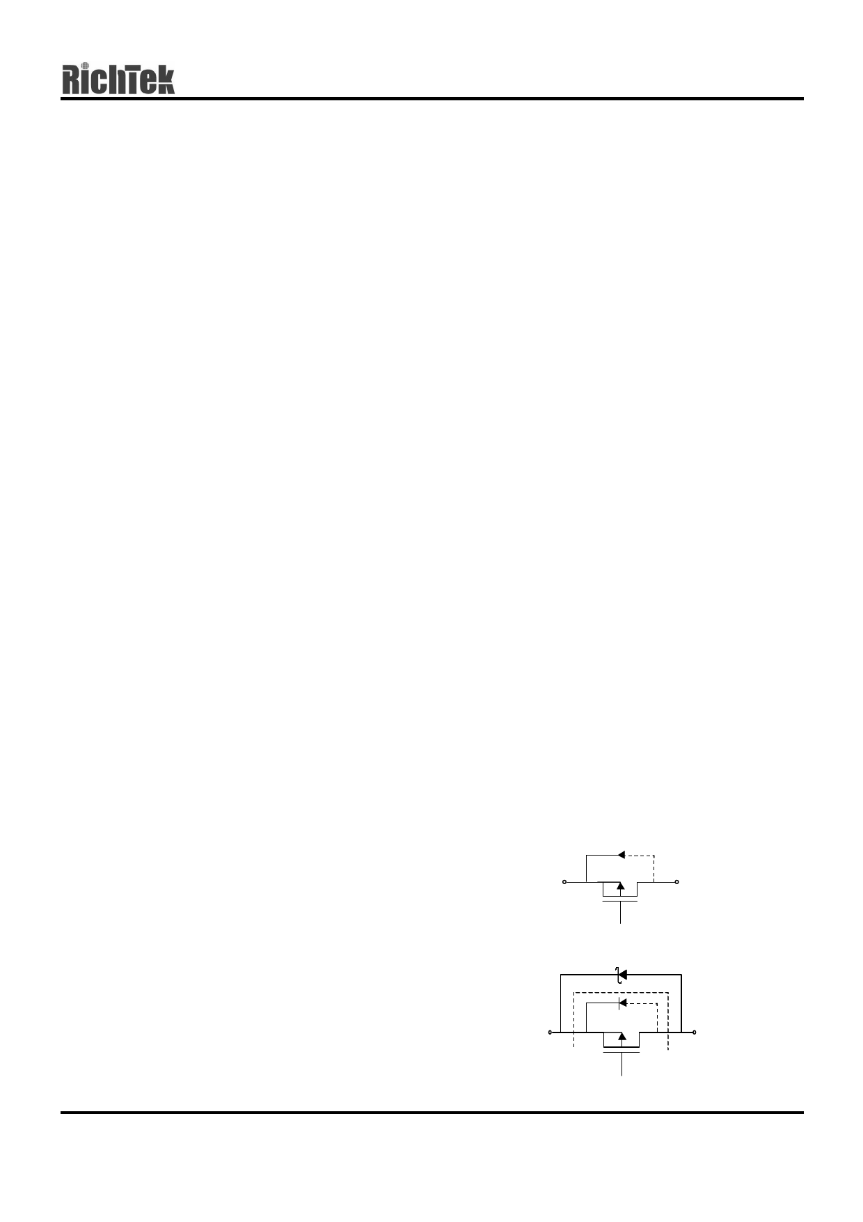
Reverse Current Path
The power transistor used in the RT9181 has an
inherent diode connected between each regulator
input and output (see Fig.1). If the output is forced
above the input by more than a diode-drop, this diode
will become forward biased and current will flow from
the VOUT terminal to VIN. This diode will also be
turned on by abruptly stepping the input voltage to a
value below the output voltage. To prevent regulator
mis-operation, a Schottky diode could be used in the
applications where input/output voltage conditions
can cause the internal diode to be turned on (see
Fig.2). As shown, the Schottky diode is connected in
parallel with the internal parasitic diode and prevents
it from being turned on by limiting the voltage drop
across it to about 0.3V < 100mA to prevent damage
to the part.
Fig. 1
VIN
VOUT
Fig. 2
www.richtek-ic.com.tw
7
Share Link: 