CY2309SXC-1(2008) Ver la hoja de datos (PDF) - Cypress Semiconductor
Número de pieza
componentes Descripción
Lista de partido
CY2309SXC-1 Datasheet PDF : 15 Pages
| |||
CY2305
CY2309
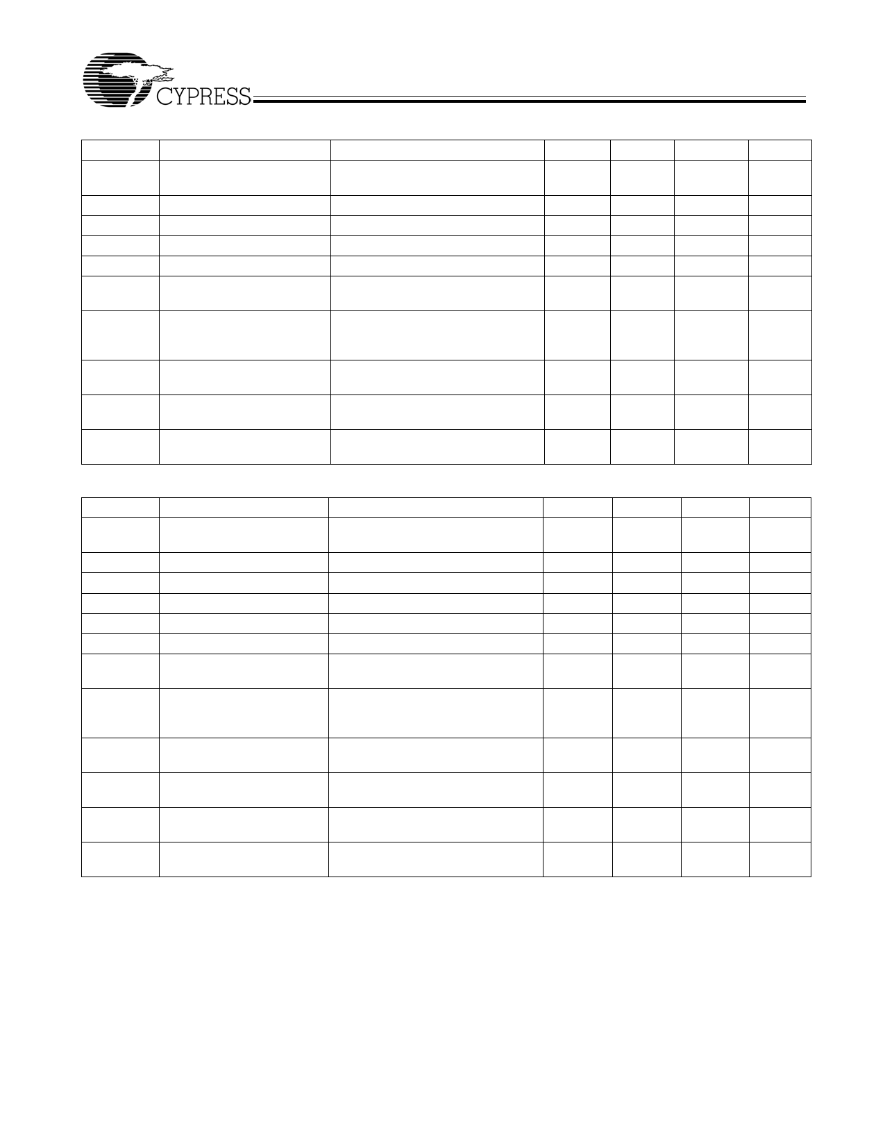
Electrical Characteristics for CY2305SI-XX and CY2309SI-XX Industrial Temperature Devices
Parameter
VIL
VIH
IIL
IIH
VOL
Description
Input LOW Voltage[5]
Input HIGH Voltage[5]
Input LOW Current
Input HIGH Current
Output LOW Voltage[6]
VOH
Output HIGH Voltage[6]
IDD (PD mode) Power down Supply Current
IDD
Supply Current
Test Conditions
Min
–
2.0
VIN = 0V
–
VIN = VDD
–
IOL = 8 mA (–1)
–
IOH =12 mA (–1H)
IOH = –8 mA (–1)
2.4
IOL = –12 mA (–1H)
REF = 0 MHz
–
Unloaded outputs at 66.67
–
MHz, SEL inputs at VDD
Max
Unit
0.8
V
–
V
50.0
μA
100.0
μA
0.4
V
–
V
25.0
μA
35.0
mA
Switching Characteristics for CY2305SI-1 and CY2309SI-1 Industrial Temperature Devices
Parameter[7]
Name
Test Conditions
Min
Typ. Max Unit
t1
Output Frequency
30 pF load
10 pF load
10
– 100 MHz
10
133.33 MHz
tDC
Duty Cycle[6] = t2 ÷ t1
Measured at 1.4V, Fout = 66.67 MHz
40.0
50.0 60.0
%
t3
Rise Time[6]
Measured between 0.8V and 2.0V
–
– 2.50
ns
t4
Fall Time[6]
Measured between 0.8V and 2.0V
–
– 2.50
ns
t5
Output to Output Skew[6] All outputs equally loaded
–
85 250
ps
t6A
Delay, REF Rising Edge to
CLKOUT Rising Edge[6]
Measured at VDD/2
–
– ±350 ps
t6B
Delay, REF Rising Edge to
CLKOUT Rising Edge[6]
Measured at VDD/2. Measured in PLL
Bypass Mode, CY2309 device only.
1
5 8.7
ns
t7
tJ
tLOCK
Device to Device Skew[6] Measured at VDD/2 on the CLKOUT pins
–
of devices
Cycle to Cycle Jitter[6] Measured at 66.67 MHz, loaded outputs
–
PLL Lock Time[6]
Stable power supply, valid clock
–
presented on REF pin
– 700
ps
70 200
ps
– 1.0
ms
Switching Characteristics for CY2305SI-1H and CY2309SI-1H Industrial Temperature Devices
Parameter[7]
Name
Description
Min
Typ. Max Unit
t1
Output Frequency
30 pF load
10 pF load
10
– 100 MHz
10
133.33 MHz
tDC
Duty Cycle[6] = t2 ÷ t1
Measured at 1.4V, Fout = 66.67 MHz
40.0
50.0 60.0
%
t3
Rise Time[6]
Measured between 0.8V and 2.0V
–
– 1.50
ns
t4
Fall Time[6]
Measured between 0.8V and 2.0V
–
– 1.50
ns
t5
Output to Output Skew[6] All outputs equally loaded
–
85 250
ps
t6A
Delay, REF Rising Edge to
CLKOUT Rising Edge[6]
Measured at VDD/2
–
– ±350 ps
t6B
Delay, REF Rising Edge to
CLKOUT Rising Edge[6]
Measured at VDD/2. Measured in PLL
Bypass Mode, CY2309 device only.
1
5 8.7
ns
t7
Device to Device Skew[6] Measured at VDD/2 on the CLKOUT pins
–
– 700
ps
of devices
Document #: 38-07140 Rev. *I
Page 6 of 15
[+] Feedback
Share Link: 