CY7C4201V(2003) Ver la hoja de datos (PDF) - Cypress Semiconductor
Número de pieza
componentes Descripción
Lista de partido
CY7C4201V Datasheet PDF : 17 Pages
| |||
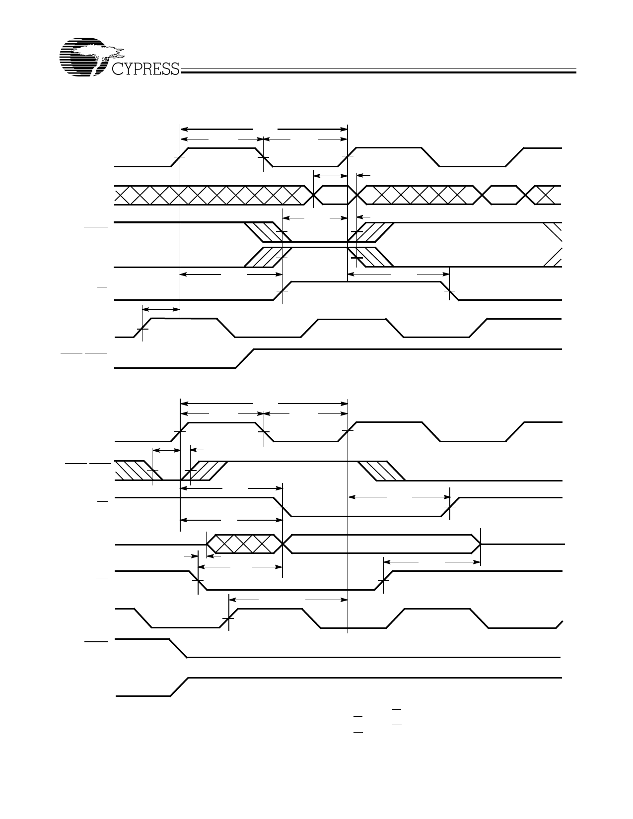
Switching Waveforms
Write Cycle Timing
WCLK
D0 –D8
WEN1
tCLKH
tCLK
tCLKL
tDS
tENS
WEN2
(if applicable)
FF
RCLK
tWFF
[11]
tSKEW1
REN1,REN2
Read Cycle Timing
RCLK
REN1,REN2
tENS
EF
Q0 –Q8
OE
tOLZ
WCLK
WEN1
tCLKH
tCKL
tCLKL
tENH
tREF
tA
NO OPERATION
tOE
[12]
tSKEW1
CY7C4421V/4201V/4211V/4221V
CY7C4231V/4241V/4251V
tDH
tENH
tWFF
NO OPERATION
NO OPERATION
tREF
VALID DATA
tOHZ
WEN2
Notes:
11. tSKEW1 is the minimum time between a rising RCLK edge and a rising WCLK edge to guarantee that FF will go HIGH during the current clock cycle. If the time between the rising
edge of RCLK and the rising edge of WCLK is less than tSKEW1, then FF may not change state until the next WCLK rising edge.
12. tSKEW1 is the minimum time between a rising WCLK edge and a rising RCLK edge to guarantee that EF will go HIGH during the current clock cycle. It the time between the rising
edge of WCLK and the rising edge of RCLK is less than tSKEW1, then EF may not change state until the next RCLK rising edge.
Document #: 38-06010 Rev. *A
Page 9 of 17
Share Link: 