EM4006F9WT7E Ver la hoja de datos (PDF) - EM Microelectronic - MARIN SA
Número de pieza
componentes Descripción
Lista de partido
EM4006F9WT7E
EM Microelectronic - MARIN SA

EM4006F9WT7E Datasheet PDF : 10 Pages
| |||
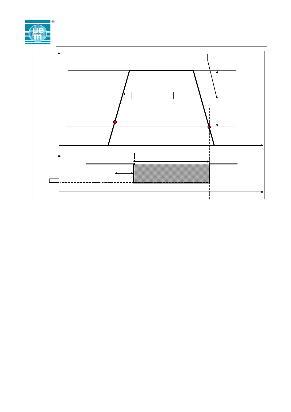
supply voltage
VDD
chip operating voltage range: from Vmin to Vmax
Vmax (voltage clipping)
EM4006
chip supply voltage
Vr (Read wake up)
Vmin
modulator
ON/OFF
ON
OFF
64 bits
period
Miller Encoder
The input to Miller encoder is NRZ data coming from
LROM. The output is coded according to Miller format and
is driving the modulator Switch. See figure 6 for example
of Miller code.
Clock Generation
The clock of the logic is extracted from the RF signal. The
clock extracted from RF signal is driving the divider chain
consisting of toggle flip-flops. The output of this divider
chain is data clock with which the data from Laser ROM
(LROM) is addressed, encoded and sent to Modulator
Switch.
The layout of divider chain is designed in a way that
different data rates can be chosen with metal mask
(options).
The following division factors are possible on request:
128, 256, 1024, 2048, 4094 and 8192.
The standard is 512.
time
READ
time
Fig. 7
Others
As mentioned in Output Sequence, during the pause (LW)
the Modulator Switch is OFF. When observing the pause
duration one has to remember that the time with
Modulator Switch OFF effectively observed can vary due
to different terminations of STDMS. The stop bit at 0 can
be represented either by Modulator Switch ON or OFF
depending on the data. The start bit at 1 adds 1/2 of data
period OFF (transition in the middle of bit period).
Figure below show the four possible terminations of
STDMS and its influence on entire period passed by
Modulator Switch OFF. Level LOW represents Modulator
Switch OFF. LDB stands for last data bit.
Copyright 2001, EM Microelectronic-Marin SA
7
www.emmicroelectronic.com
Share Link: