AV9169AM-70 Ver la hoja de datos (PDF) - Integrated Circuit Systems
Número de pieza
componentes Descripción
Lista de partido
AV9169AM-70 Datasheet PDF : 7 Pages
| |||
ICS9169A-70
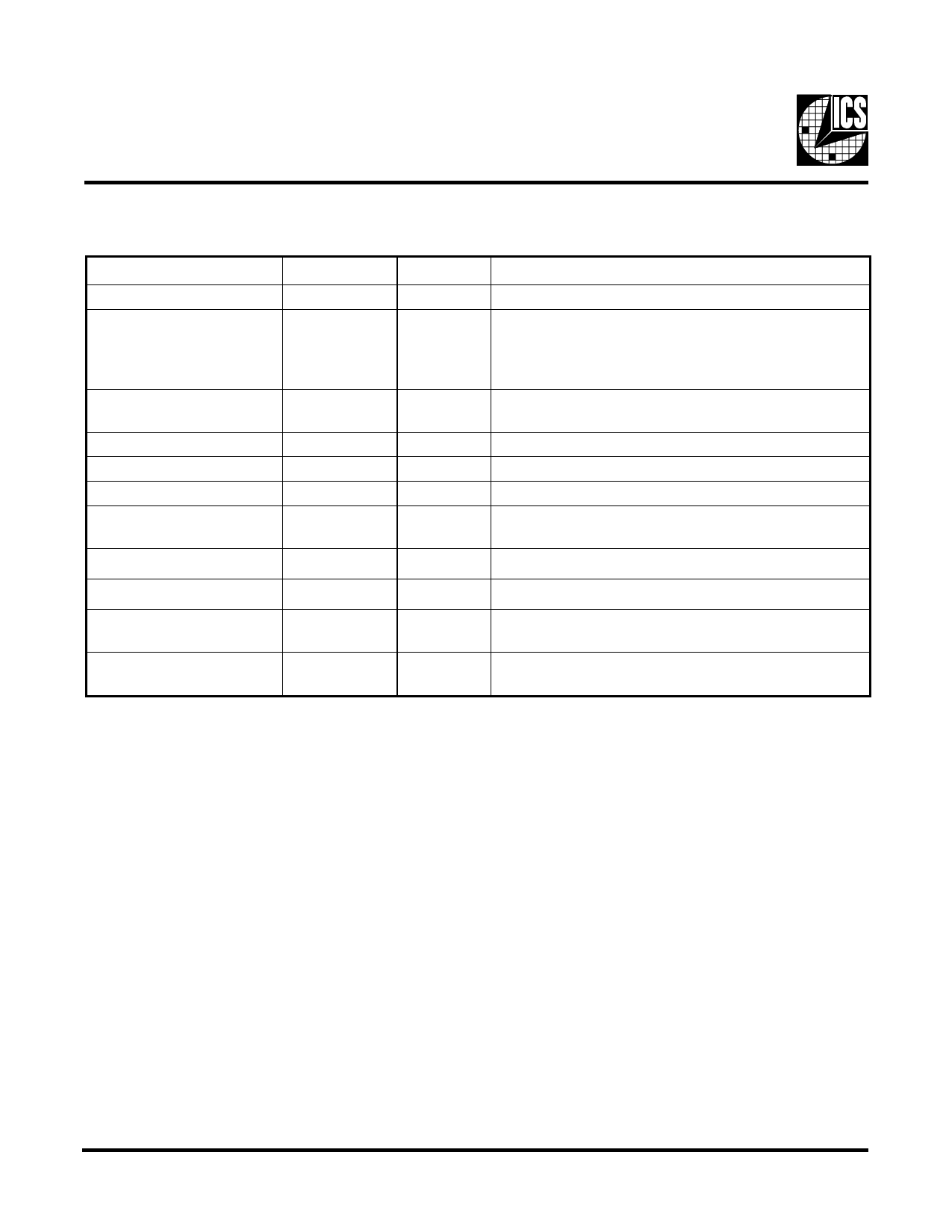
Pin Descriptions
PIN NUMBER
1
2
PIN NAME
VDD1
X1
3
X2
5,6,9,10,13,14,20,23,24
4,7,11,19,22,25
8,12,21
PCI(0:8)
GND
VDD3
15,16,17
FS(0:2)A
29
28,27,26
VDD2
SCSI (0:2)
31,30,18
FS(0:2)B
32
REF0
TYPE
PWR
IN
OUT
OUT
PWR
PWR
IN
PWR
OUT
IN
OUT
DESCRIPTION
Power for logic, PLL and output buffers.
XTAL or external reference frequency input. This
input includes XTAL load capacitance and feedback
bias for a 12-16 MHz crystal, nominally 14.31818
Mhz.
XTAL output which includes XTAL load
capacitance.
PCI clock outputs
Ground for logic, PLL and output buffers.
Power for PCI clock outputs
Frequency multiplier select pins. See table above.
These inputs have internal pull up devices.
Power for SCSI clock outputs
SCSI clock outputs
Frequency multiplier select pins. See table next
page. These inputs have internal pull up devices
REF is a buffered copy of the crystal oscillator or
reference input clock, nominally 14.31818 MHz.
Note:
X1, X2 contain iternal 18pF crystal load cap. Intended to have external load
caps of 15 to 18pF required for nominal crystal of 17 to 18pF crystal total load.
2
Share Link: 