IMP37 Ver la hoja de datos (PDF) - IMP, Inc
Número de pieza
componentes Descripción
Lista de partido
IMP37 Datasheet PDF : 6 Pages
| |||
IMP37
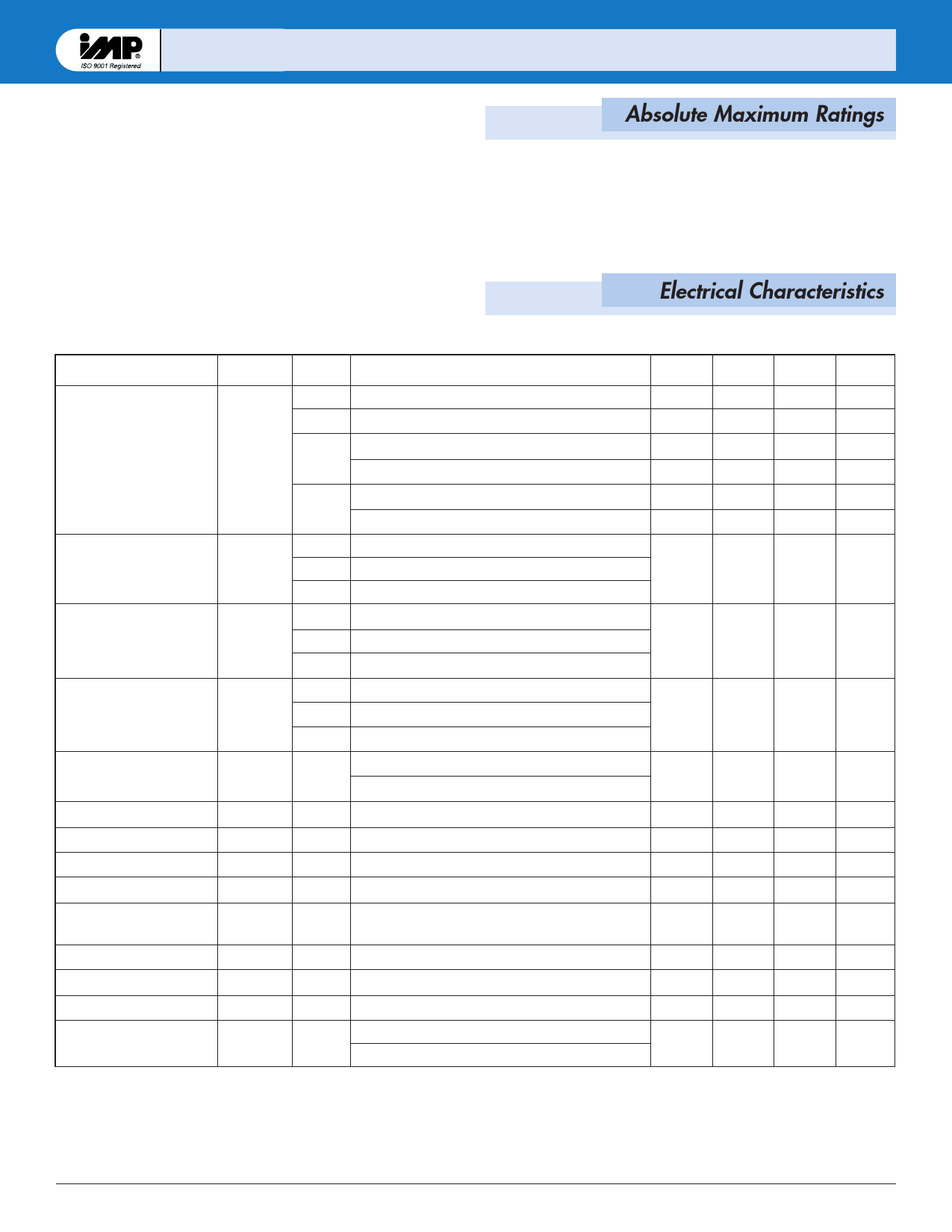
Absolute Maximum Ratings
Input Voltage . . . . . . . . . . . . . . . . . . . . . . . . . 7V
Operating Junction Temperature . . . . . . . . . 0°C to 150°C
Storage Temperature Range . . . . . . . . . . . . . –65°C to +150°C
Lead Temperature (Soldering) . . . . . . . . . . . . . 300°C for 10 seconds
These are stress ratings only and functional operation is not implied.
Exposure to absolute maximum ratings for prolonged time periods may
affect device reliability. All voltages are with respect to ground.
Electrical Characteristics
Specifications apply over the junction operating temperature range of TJ = 0°C to +125°C unless otherwise noted.
Parameter
Symbol Suffix Conditions
Min Typ Max Units
Output Voltage
VOUT
–25 IOUT = 10mA, VIN = 4.85V, TJ = 25°C
10mA ≤ IOUT ≤ IMAX, 4.25V ≤ VIN ≤ 5.5V
2.475
2.45
–30 IOUT = 10mA, VIN = 5V, TJ = 25°C
2.97
10mA ≤ IOUT ≤ IMAX, 4.75V ≤ VIN ≤ 5.5V
2.94
–33 IOUT = 10mA, VIN = 5V, TJ = 25°C
3.267
10mA ≤ IOUT ≤ IMAX, 4.75V ≤ VIN ≤ 5.5V
3.235
Line Regulation
(Note 1)
Line Regulation
(Note 1)
–25 IOUT = 10mA, 4.25V ≤ (VIN) ≤ 5.5V
–30 IOUT = 10mA, 4.5V ≤ VIN ≤ 5.5V
–33 IOUT = 10mA, 4.5V ≤ VIN ≤ 5.5V
–25 IOUT = 10mA, 4.25V ≤ (VIN) ≤ 5.5V, TA = 25°C
–30 IOUT = 10mA, 4.5V ≤ VIN ≤ 5.5V, TA = 25°C
–33 IOUT = 10mA, 4.5V ≤ VIN ≤ 5.5V, TA = 25°C
Load Regulation
(Note 1)
–25 VIN = 4.25V, 5mA ≤ IOUT ≤ 800mA
–30 VIN = 4.75V, 5mA ≤ IOUT ≤ 800mA
–33 VIN = 4.75V, 5mA ≤ IOUT ≤ 800mA
Dropout Voltage
(Note 2)
–xx IOUT = 100mA
IOUT = 800mA
Current Limit
IOUT(MAX) –xx TJ = 25°C
800
Minimum Load Current
–xx
Quiescent Current
IQ
–xx VIN ≤ 6V
Thermal Regulation
TA = 25°C, 30ms Pulse
Ripple Rejection
fRIPPLE = 120Hz, VIN = 5V, TA = 25°C
51
VRIPPLE = 1Vp-p, ILOAD= 10mA
Temperature Stability
2.5
2.5
3.00
3.00
3.30
3.30
12
12
12
2.8
2.8
2.8
25
25
25
950
36
0.01
54
0.5
2.525
2.55
3.03
3.06
3.333
3.365
19
19
19
4.3
4.3
4.3
30
30
30
0.8
0.95
1200
5.0
75
0.1
V
mV
mV
mV
V
mA
mA
µA
%/W
dB
%
Long Term Stability
RMS Output Noise
Thermal Resistance
TA = 125°C, 1000 Hrs
(% of VOUT), 10Hz ≤ f ≤ 10kHz, TJ = 25°C
Junction-to-Case at TAB (TO-223)
0.3
0.003
15
Junction-to-Case at TAB (TO-263)
10
Notes: 1. See thermal regulation specification for changes in output voltage due to heating effects. Load regulation and line regulation
are measured with low duty cycle pulse testing to maintain a constant junction temperature.
2. Dropout voltage is specified over the full output current range. Dropout voltage is defined as the minimum input/output
differential measured at the specified output current.
3. Minimum load current is defined as the minimum output current required to maintain regulation.
%
%
°C/W
37_t07.eps
© 1999 IMP, Inc.
408-432-9100/www.impweb.com
3
Share Link: 