PI90LVT211 Ver la hoja de datos (PDF) - Pericom Semiconductor
Número de pieza
componentes Descripción
Lista de partido
PI90LVT211 Datasheet PDF : 9 Pages
| |||
PI90LV211/PI90LVT211
1:6 Differential Clock
Distribution Chip 1122334455667788990011223344556677889900112233445566778899001122112233445566778899001122334455667788990011223344556677889900112211223344556677889900112233445566778899001122334455667788990011221122334455667788990011223344556677889900112233445566778899001122112233445566778899001122
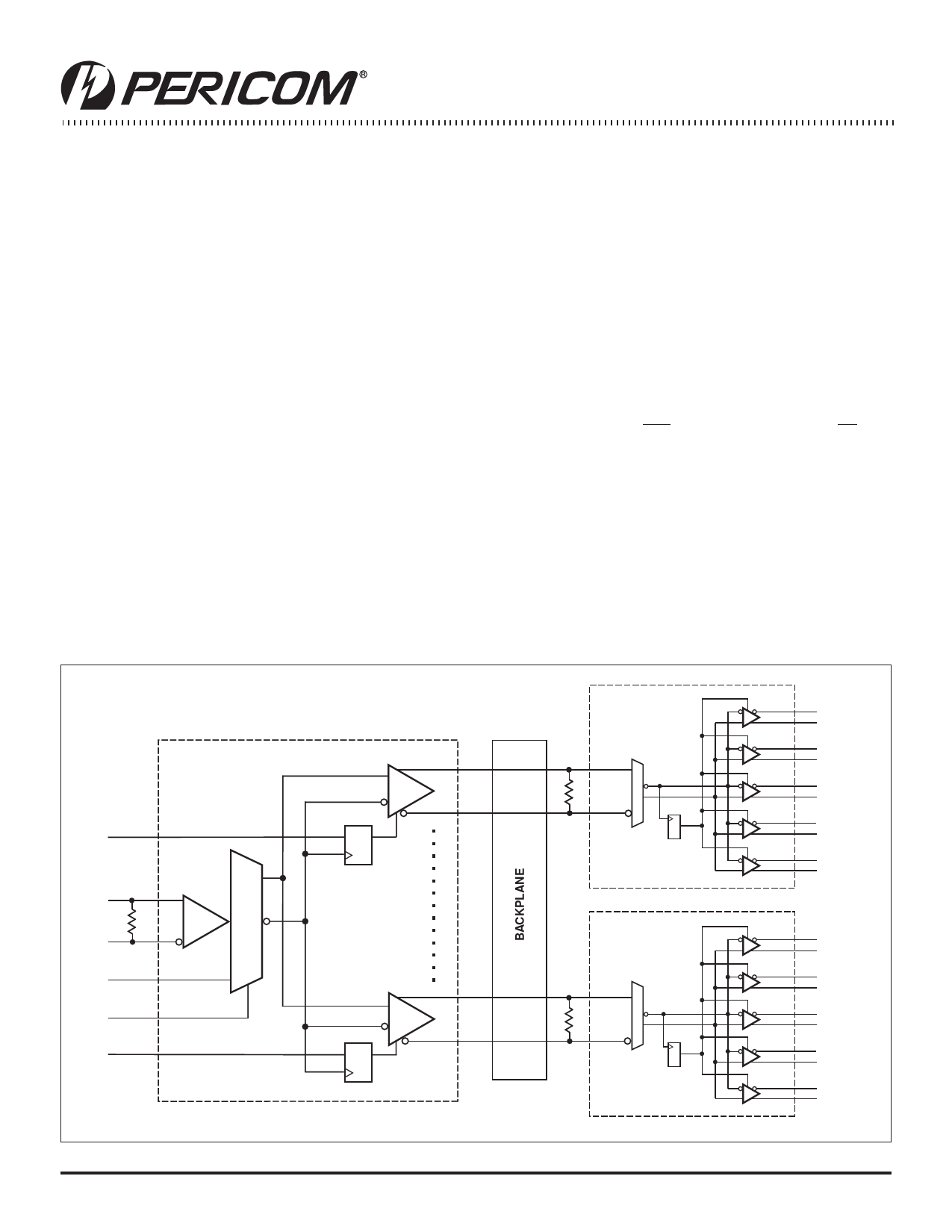
General Desciption
The PI90LV211 is a 1:6 fanout tree designed explicitly for low-skew,
high-speed clock distribution. The device was targeted to work in
conjunction with the PI90LV14 device to provide another level of
flexibility in the design and implementation of clock distribution
trees. The individual synchronous enable controls and multiplexed
clock inputs make the device ideal as the first level distribution unit
in a distribution tree. The device provides the ability to distribute
a lower speed scan or test clock along with the high-speed system
clock to ease the design of system diagnostics and self test
procedures. The individual enables could be used to allow for the
disabling of individual cards on a backplane in fault tolerant
designs.
Handling Open Inputs and Outputs
With the simultaneous switching characteristics and the tight skew
specifications of the P90LV211, the handling of the unused outputs
becomes critical. To minimize the noise generated on the die
all outputs should be terminated in pairs, i.e. both the true and
compliment outputs should be terminated even if only one of the
outputs will be used in the system. With both complimentary pairs
terminated, the current in the VCC pins will remain essentially
constant and thus inductance induced voltage glitches on VCC will
not occur. VCC glitches will result in distorted output waveforms
and degradations in the skew performance of the device.
The package parasitics of the 28-lead package cause the signals on
a given pin to be influenced by signals on adjacent pins. PI90LV211
is characterized and tested with all of the outputs switching,
therefore the numbers in the data book are guaranteed only for this
situation. If all of the outputs of the PI90LV211 are not needed and
there is a desire to save power, the unused output pairs can be left
unterminated. Unterminated outputs can influence the propagation
delay on adjacent pins by 15ps–20ps. Therefore, under these
conditions, this 15ps–20ps needs to be added to the overall skew
of the device. Pins which are separated by a package corner are not
considered adjacent pins in the context of propagation delay
influence. Therefore if all of the outputs on a single side of the
package are terminated, the specification limits in the data sheet will
apply.
Using the Enable Pins
Both the common enable (CEN) and the individual enables (ENx) are
synchronous to the CLK or SCLK input depending on which is
selected. The active low signals are clocked into the enable flip flops
on the negative edges of the PI90LV211 clock inputs. In this way,
the devices will only be disabled when the outputs are already in the
LOW state. The internal propagation delays are such that the delay
to the output through the distribution buffers is less than that
through the enable flip flops. This will ensure that the disabling of
the device will not slice any time off the clock pulse. On initial power
up, the enable flip flops will randomly attain a stable state; therefore
precautions should be taken on initial power up to ensure the
PI90LV211 is in the desired state.
PI90LV211
D0
PI90LV14
PI90LV14
D5
Figure 8. Standard PI90LV211 LVDS Application
7
PS8535C 10/04/04
Share Link: 