MAX8559(2004) Ver la hoja de datos (PDF) - Maxim Integrated
Número de pieza
componentes Descripción
Lista de partido
MAX8559
(Rev.:2004)
(Rev.:2004)
Maxim Integrated

MAX8559 Datasheet PDF : 12 Pages
| |||
19-3121; Rev 0; 1/04
EVAALVUAAILTAIOBNLEKIT
Dual, 300mA, Low-Noise Linear Regulator
with Independent Shutdown in UCSP or TDFN
General Description
The MAX8559 dual, low-noise, low-dropout (LDO) linear
regulator operates from a 2.5V to 6.5V input voltage
and delivers at least 300mA of continuous output cur-
rent. It offers low output noise and low dropout of only
60mV at 100mA. Typical output noise for this device is
32µVRMS, and PSRR is 70dB at 10kHz. Designed with
an internal P-channel MOSFET pass transistor, the
MAX8559 maintains a low 115µA supply current per
LDO, independent of the load current and dropout volt-
age. Other features include short-circuit protection and
thermal-shutdown protection. The MAX8559 includes
two independent logic-controlled shutdown inputs and
is capable of operating without a bypass capacitor to
further reduce total solution size. The MAX8559 is avail-
able in a miniature 8-bump UCSP (2mm x 1mm) or
8-pin TDFN (3mm x 3mm) package.
Applications
Cellular and Cordless Phones
PDAs and Palmtop Computers
Notebook Computers
Digital Cameras
PCMCIA Cards
Wireless LAN Cards
Hand-Held Instruments
Features
♦ Two Low-Dropout-Voltage Regulators
♦ Low 32µVRMS Output Noise
♦ 300mA Output Current for Each LDO
♦ 70dB PSRR at 10kHz
♦ Independent Shutdown Controls
♦ Low 60mV Dropout at 100mA Load
♦ 115µA Operating Supply Current per LDO
♦ 1.5V to 3.3V Factory-Preset Output
♦ Small Ceramic Output Capacitors
♦ Output Current Limit
♦ Thermal-Overload and Short-Circuit Protection
♦ 1.95W Power-Dissipation Capability (TDFN)
♦ 2mm2 Footprint (UCSP)
Ordering Information
PART
TEMP RANGE
PIN-PACKAGE
MAX8559EBAxy*† -40°C to +85°C
8 UCSP (B8-1)
MAX8559ETAxy*
-40°C to +85°C
8 TDFN-EP**
*xy = Output voltage code (see the Output Voltage
Selector Guide).
**EP = Exposed pad.
†Future product—contact factory for availability.
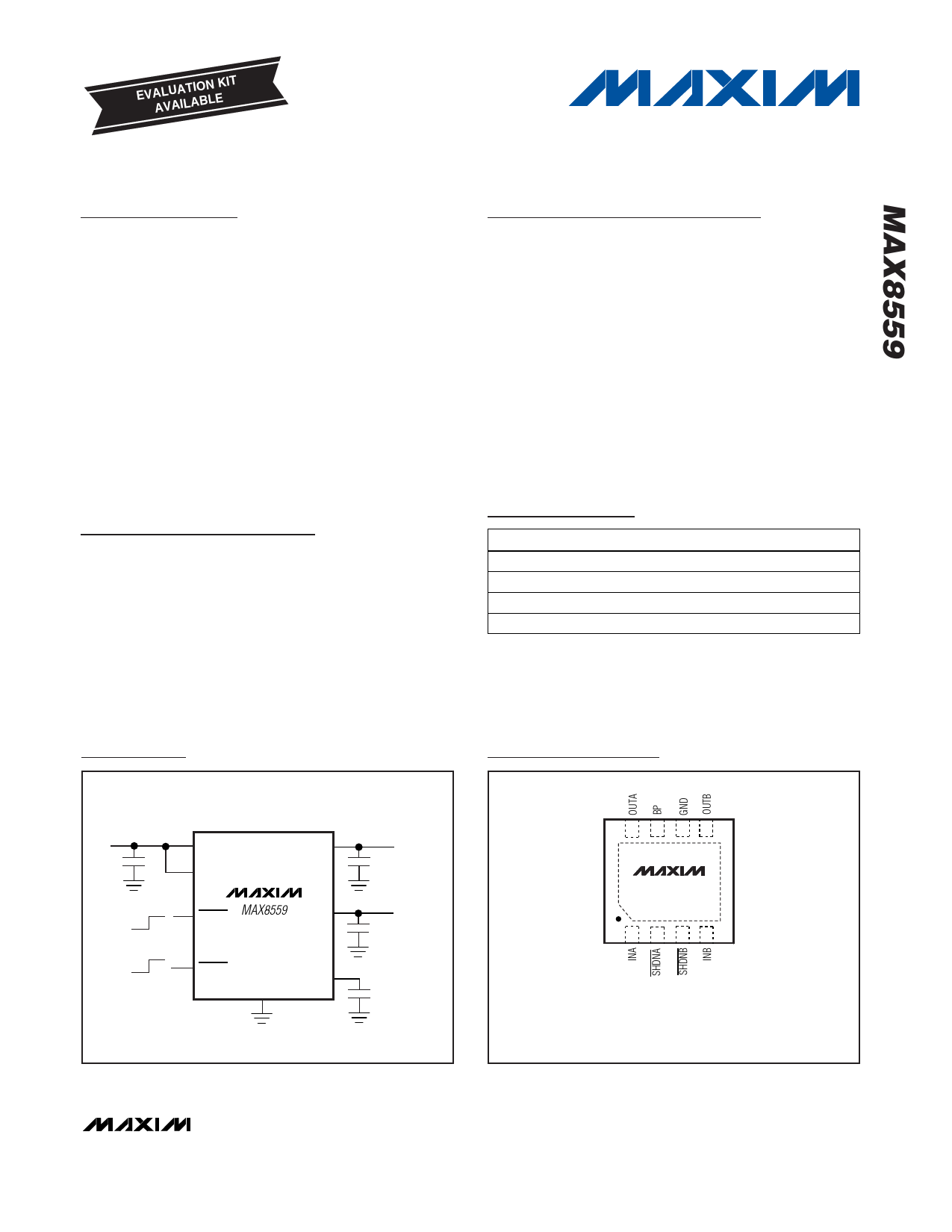
Typical Operating Circuit
Pin Configurations
INPUT
2.5V TO 6.5V
2.2µF
min
ON
OFF
ON
OFF
INA
OUTA
INB
SHDNA MAX8559 OUTB
SHDNB
BP
GND
1.5V TO 3.3V
2.2µF/150mA
4.7µF/300mA
1.5V TO 3.3V
2.2µF/150mA
4.7µF/300mA
0.01µF
(OPTIONAL)
TOP VIEW
8 7 65
MAX8559ETA
1 2 34
TDFN
3mm x 3mm
Pin Configurations continued at end of data sheet.
Output Voltage Selector Guide appears at end of data sheet.
________________________________________________________________ Maxim Integrated Products 1
For pricing, delivery, and ordering information, please contact Maxim/Dallas Direct! at
1-888-629-4642, or visit Maxim’s website at www.maxim-ic.com.
Share Link: