MC74HC354 Ver la hoja de datos (PDF) - Motorola => Freescale
Número de pieza
componentes Descripción
Lista de partido
MC74HC354
Motorola => Freescale

MC74HC354 Datasheet PDF : 9 Pages
| |||
MC54/74HC354
PIN DESCRIPTIONS
D0–D7 (Pins 8–1) DATA INPUTS
These eight data bits are stored in a transparent latch when
the Data–Latch Enable pin is active (high). Once enabled,
changing inputs will not change the contents of the latch.
A0, A1, A2 (Pins 14,13,12) ADDRESS INPUTS
Selects which data bit stored in the Data Latch is routed to
the outputs Y and Y.
DATA–LATCH ENABLE (Pin 9)
The latch is transparent to D0–D7 when enable is inactive
(low). The Data–Latch contents are unaffected when enable
is held active (high).
ADDRESS–LATCH ENABLE (Pin 11)
The latch is transparent to A0, A1 and A2 when enable is
inactive (low). The Address–Latch contents are unaffected
when enable is held active (high).
OE1, OE2, OE3 (Pins 15,16,17) OUTPUT ENABLES
Any of the output enable pins inactive (OE1=High or
OE2=High or OE3=Low) causes the outputs (Y and Y) to be
in high–impedance states.
Y, Y (Pins 19,18)
These 3–state outputs (when not 3–stated) represent the
data bit in the Data Latch selected by the Address Latch.
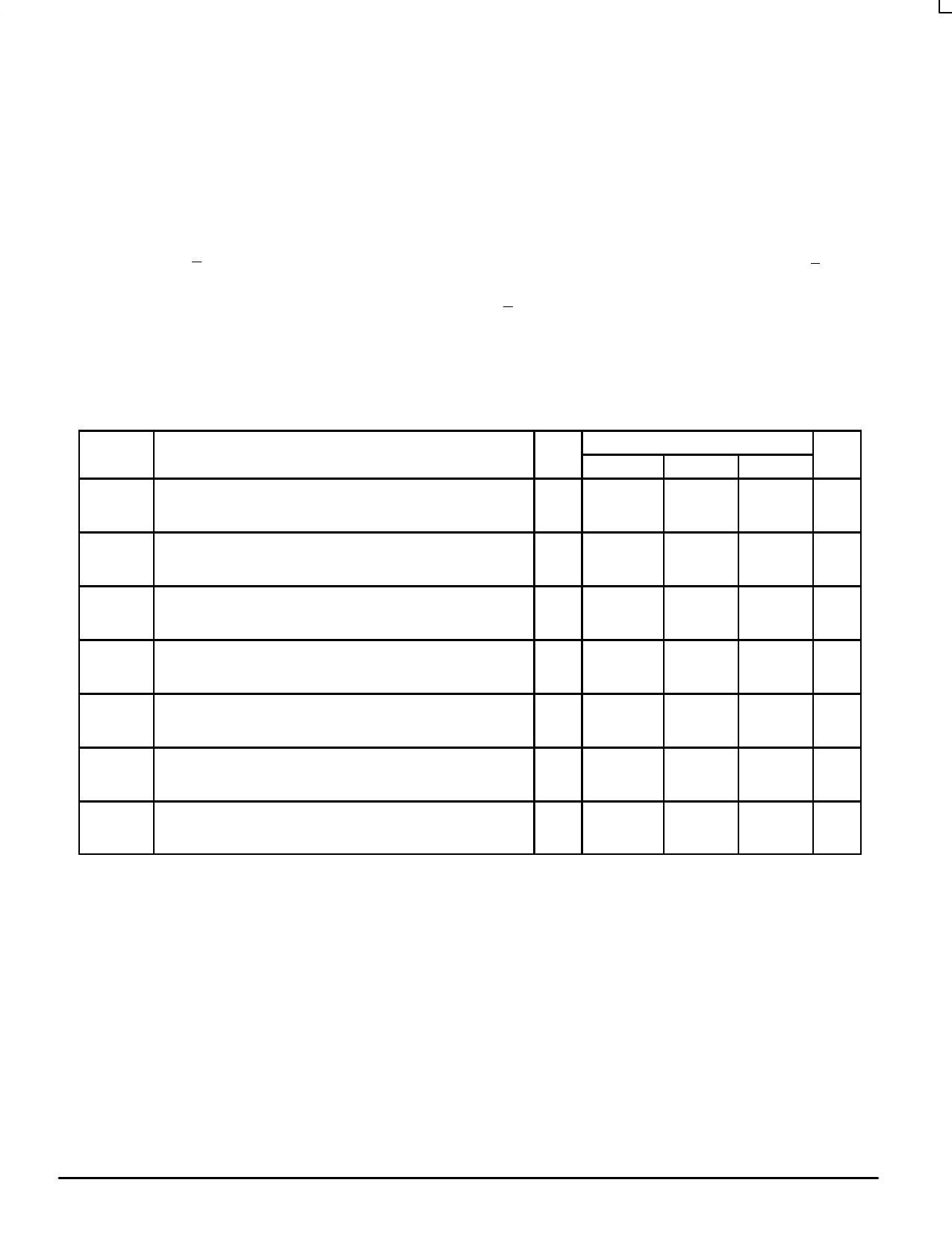
TIMING REQUIREMENTS (Input tr = tf = 6 ns)
Symbol
Parameter
VCC
Guaranteed Limit
V –55 to 25°C ≤85°C
≤125°C Unit
tsu
Minimum Setup Time, D0–D7 to Data–Latch Enable
(Figure 5)
2.0
50
4.5
10
6.0
9
65
75
ns
13
15
11
13
tsu
Minimum Setup Time, A0–A2 to Address–Latch Enable
(Figure 5)
2.0
50
4.5
10
6.0
9
65
75
ns
13
15
11
13
th
Minimum Hold Time, Data–Latch Enable to D0–D7
(Figure 5)
2.0
5
4.5
5
6.0
5
5
5
ns
5
5
5
5
th
Minimum Hold Time, Address–Latch Enable to A0–A2
(Figure 5)
2.0
5
4.5
5
6.0
5
5
5
ns
5
5
5
5
tw
Minimum Pulse Width, Data–Latch Enable
(Figure 3)
2.0
80
4.5
16
6.0
14
100
120
ns
20
24
17
20
tw
Minimum Pulse Width, Address–Latch Enable
(Figure 3)
2.0
80
4.5
16
6.0
14
100
120
ns
20
24
17
20
tr, tf
Maximum Input Rise and Fall Times
(Figure 1)
2.0
1000
1000
1000
ns
4.5
500
500
500
6.0
400
400
400
NOTE: Information on typical parametric values can be found in Chapter 2 of the Motorola High–Speed CMOS Data Book (DL129/D).
MOTOROLA
4
High–Speed CMOS Logic Data
DL129 — Rev 6
Share Link: