MIC4416BM4 Ver la hoja de datos (PDF) - Master Instrument Corporation
Número de pieza
componentes Descripción
Lista de partido
MIC4416BM4 Datasheet PDF : 12 Pages
| |||
MIC4416/4417
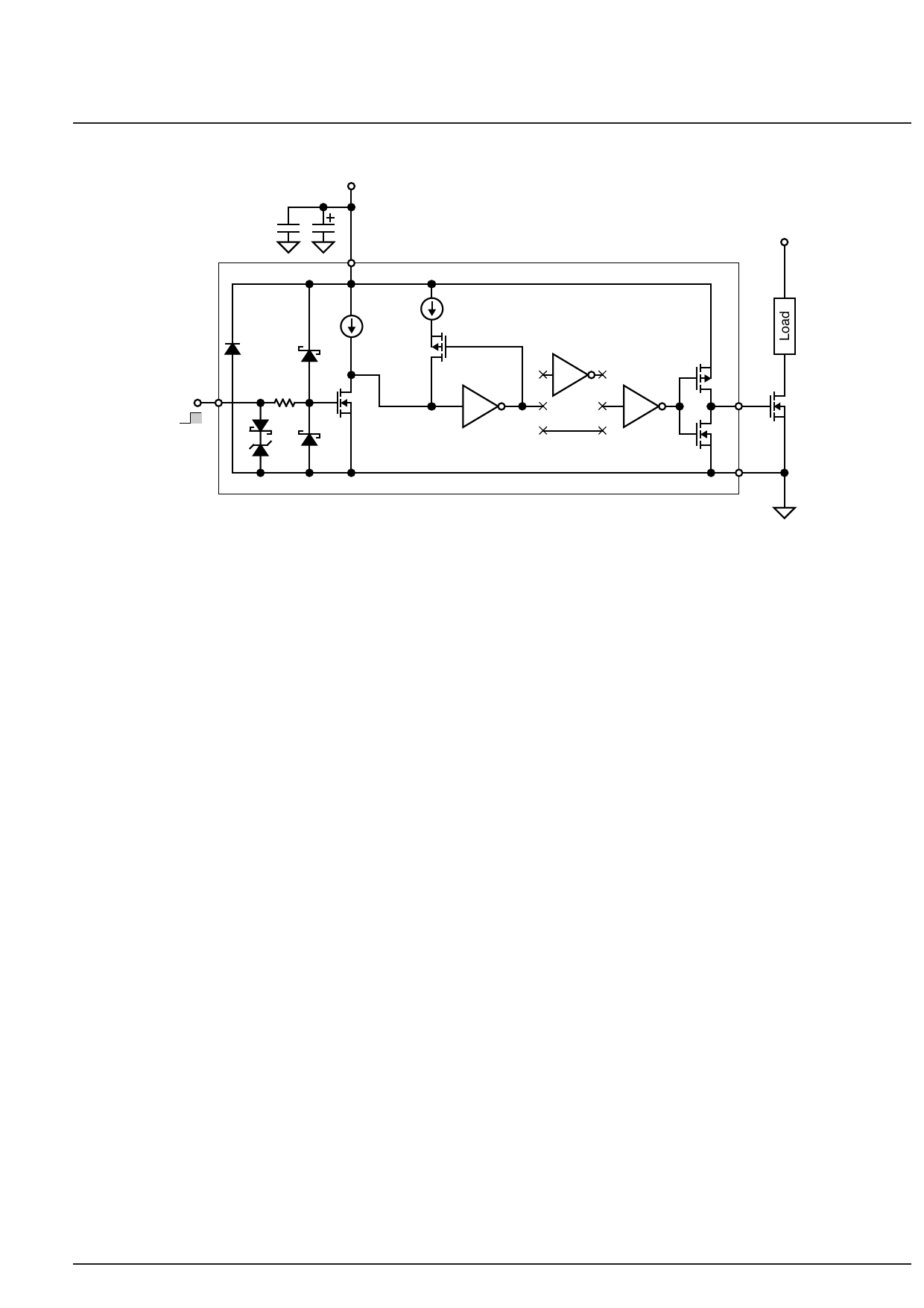
Functional Diagram
VSUPPLY
VS
Micrel, Inc.
VSWITCHED
0.3mA
0.6mA
D1
D4
Q2
R1
CTL
2k
Q1
MIC4417
INVERTING
Q3
G
Logic-Level
Input
D2
D3 D5
35V
MIC4416
Q4
NONINVERTING
GND
Functional Diagram with External Components
Functional Description
Refer to the functional diagram.
The MIC4416 is a noninverting driver. A logic high on the CTL
(control) input produces gate drive output. The MIC4417 is
an inverting driver. A logic low on the CTL (control) input
produces gate drive output. The G (gate) output is used to
turn on an external N-channel MOSFET.
Supply
VS (supply) is rated for +4.5V to +18V. External capacitors
are recommended to decouple noise.
Control
CTL (control) is a TTL-compatible input. CTL must be forced
high or low by an external signal. A floating input will cause
unpredictable operation.
A high input turns on Q1, which sinks the output of the 0.3mA
and the 0.6mA current source, forcing the input of the first
inverter low.
Hysteresis
The control threshold voltage, when CTL is rising, is slightly
higher than the control threshold voltage when CTL is falling.
When CTL is low, Q2 is on, which applies the additional
0.6mA current source to Q1. Forcing CTL high turns on Q1
which must sink 0.9mA from the two current sources. The
higher current through Q1 causes a larger drain-to-source
voltage drop across Q1. A slightly higher control voltage is
required to pull the input of the first inverter down to its
threshold.
Q2 turns off after the first inverter output goes high. This
reduces the current through Q1 to 0.3mA. The lower current
reduces the drain-to-source voltage drop across Q1. A
slightly lower control voltage will pull the input of the first
inverter up to its threshold.
Drivers
The second (optional) inverter permits the driver to be manu-
factured in inverting and noninverting versions.
The last inverter functions as a driver for the output MOSFETs
Q3 and Q4.
Gate Output
G (gate) is designed to drive a capacitive load. VG (gate
output voltage) is either approximately the supply voltage or
approximately ground, depending on the logic state applied
to CTL.
If CTL is high, and VS (supply) drops to zero, the gate output
will be floating (unpredictable).
ESD Protection
D1 protects VS from negative ESD voltages. D2 and D3
clamp positive and negative ESD voltages applied to CTL.
R1 isolates the gate of Q1 from sudden changes on the CTL
input. D4 and D5 prevent Q1’s gate voltage from exceeding
the supply voltage or going below ground.
May 2005
7
MIC4416/4417
Share Link: 