MSM7570-01 Ver la hoja de datos (PDF) - Oki Electric Industry
Número de pieza
componentes Descripción
Lista de partido
MSM7570-01 Datasheet PDF : 26 Pages
| |||
¡ Semiconductor
MSM7570-01
DEN , EXCK, DIN, DOUT
Serial control ports for MCU interface.
Reading and writing data are performed by an external MCU through these pins. Eight registers
, , witheightbitsareprovidedonthedevices.
DEN is the “Enable” control signal input, EXCK is the data shift clock input, DIN is the address
and data input, and DOUT is the data output.
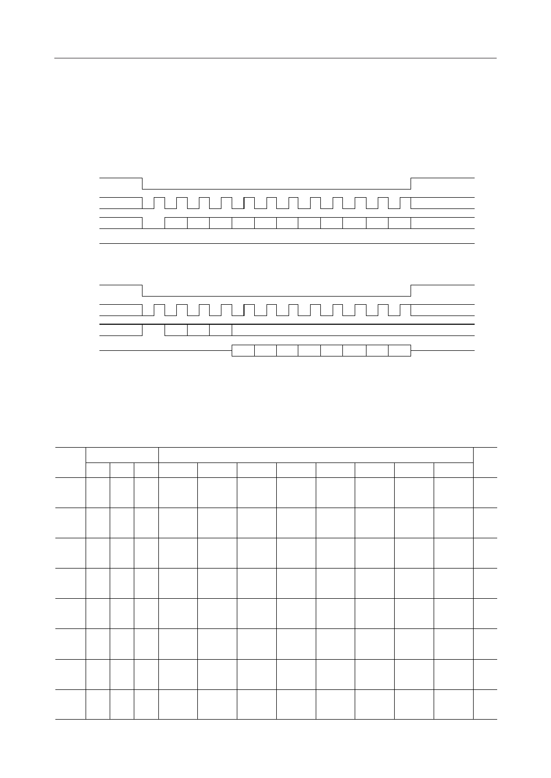
Fig.3 shows the input/output timing diagram.
DEN
EXCK
DIN
W A2 A1 A0 B7 B6 B5 B4 B3 B2 B1 B0
DOUT
High Impedance
(a) Write Data Timing Diagram
DEN
EXCK
DIN
R A2 A1 A0
DOUT
High Impedance
B7 B6 B5 B4 B3 B2 B1 B0
(b) Read Data Timing Diagram
Figure 3 MCU Interface Input/Output Timing
Table 1 shows the register map.
Table-1
Address
Control and Detect Data
Name
A2 A1 A0 B7
B6
B5
B4
B3
B2
B1
CR0 0 0 0
A/m
MCK
PDN
—
—
—
—
R/W
B0
PDN R/W
SEL
SEL
ALL
SAO/AOUT
CR1 0 0 1 MODE1 MODE0 TX
RX
TX
RX
—
RESET RESET MUTE MUTE
RX R/W
PAD
CR2 0 1 0
TX
TX
TX
TX
RX
RX
RX
RX R/W
ON/OFF GAIN2 GAIN1 GAIN0 ON/OFF GAIN2 GAIN1 GAIN0
CR3 0 1 1 Side Tone Side Tone Side Tone TONE TONE TONE TONE TONE R/W
GAIN2 GAIN1 GAIN0 ON/OFF GAIN3 GAIN2 GAIN1 GAIN0
CR4 1
0
0
DTMF/
OTHERS
TONE
SAO/
TONE4 TONE3 TONE2 TONE1 TONE0 R/W
SEL SEND VFRO
CR5 1 0 1
—
—
—
—
—
—
—
— R/W
CR6 1 1
CR7 1 1
0
VOX
ON
ON/OFF LVL1
ON
LVL0
OFF
TIME
1
VOX TX NOISE TX NOISE
—
OUT LVL1 LVL0
VOX RX NOISE RX NOISE RX NOISE
R/W
IN LEVEL SEL LVL1 LVL0
—
—
—
—R
R/W : Read/Write enable R : Read only register.
9/26
Share Link: 