PI74VCX16244V Ver la hoja de datos (PDF) - Pericom Semiconductor
Número de pieza
componentes Descripción
Lista de partido
PI74VCX16244V Datasheet PDF : 7 Pages
| |||
PI74VCX16244
1234567890123456789012345678901212345678901234567890123456789012112634-5B67I8T901B23U456F7F89E01R2345D67R89I0V121E23R456W789I0T12H345367-8S90T12A34T56E789O01U212T34P56U78T90S12
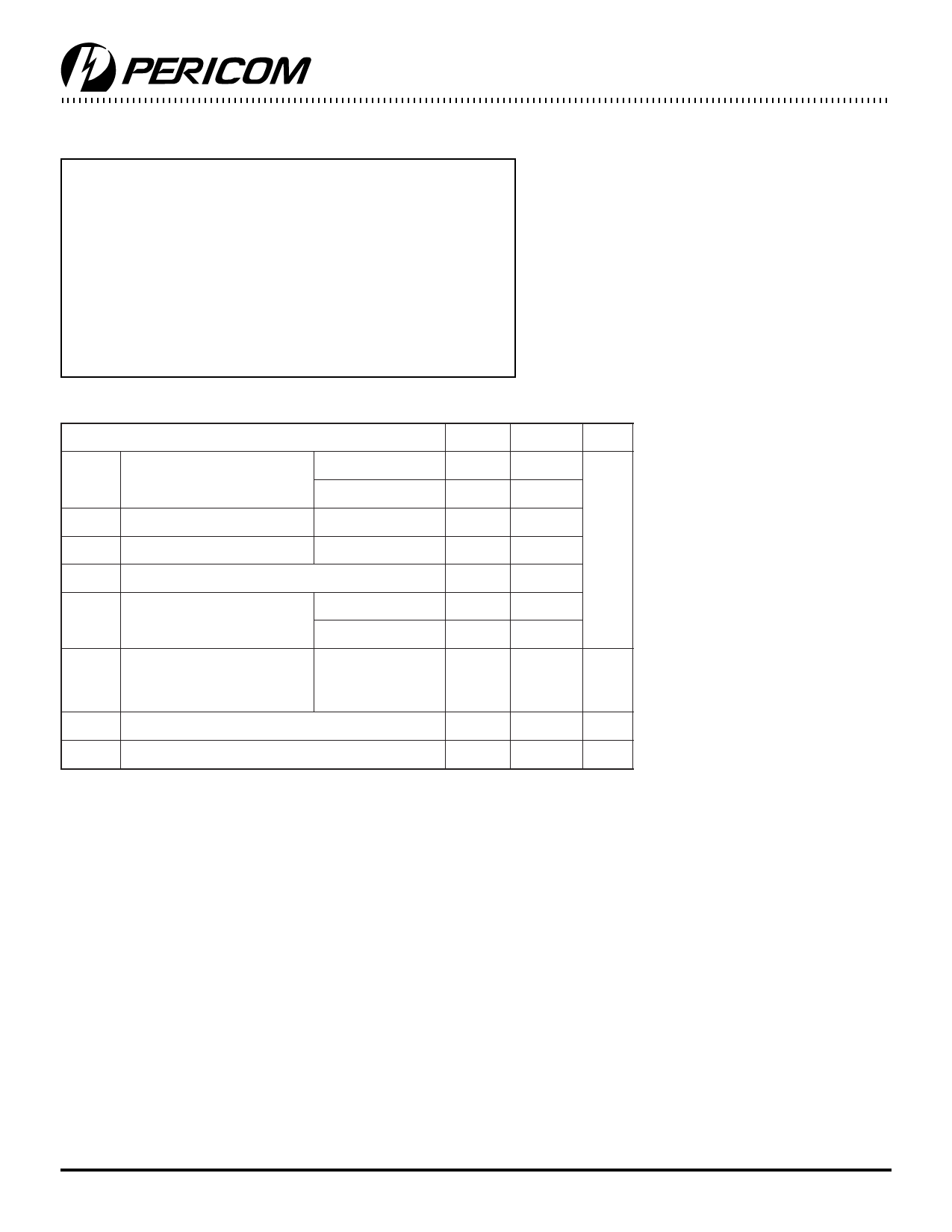
Maximum Ratings
(Above which the useful life may be impaired. For user guidelines, not tested.)
Supply Voltage Range, VDD ........................................... 0.5V to 4.6V
Input Voltage Range, VI ............................................... -0.5V to 4.6V
Output Voltage Range, VO (3-Stated) ........................... -0.5V to 4.6V
Output Voltage Range, VO(1) (Active) ..................... -0.5V to VCC+0.5
DC Input Diode Current (IIK) VI<0V ...................................... -50mA
DC Output Diode Current (IOK)
VO<0V .................................................................................. -50mA
VO>VDD ............................................................................... +50mA
DC Output Source/Sink Current (IOH/IOL) .............................. ±50mA
DC VDD or GND Current per Supply Pin (ICC or GND) ...... ±100mA
Storage Temperature Range, Tstg .............................. –65°C to 150°C
Note:
Stresses greater than those listed under MAXIMUM
RATINGS may cause permanent damage to the device.
This is a stress rating only and functional operation of the
device at these or any other conditions above those indi-
cated in the operational sections of this specification is not
implied. Exposure to absolute maximum rating conditions
for
extended periods may affect reliability.
Recommended Operating Conditions(2)
VDD Supply voltage
Operating
Data Retention Only
VIH High-level input voltage
VIL Low-level input voltage
VI Input voltage
VO Output voltage
VDD = 2.7V to 3.6V
VDD = 2.7V to 3.6V
Active State
Off State
IO
∆t/∆v
Output current in IOH/IOL
VDD = 3.0V to 3.6V
VDD = 2.3V to 2.7V
VDD = 1.8V
Input transistion rise or fall rate(3)
TA Operating free-air temperature
Min.
1.8
1.2
2.0
-0.3
0
0
0
−40
Max.
3.6
3.6
Units
0.8
V
3.6
VDD
3.6
±24
±18
mA
±6
10
ns/V
85
C
Notes
1. Absolute maximum of IO must be observed.
2. Unused control inputs must be held HIGH or LOW to prevent them from floating.
3 As measured between 0.8V and 2.0V, VDD = 3.0V.
3
PS8160A
09/09/98
Share Link: 