PI74LCX245(1997) Ver la hoja de datos (PDF) - Pericom Semiconductor Corporation
Número de pieza
componentes Descripción
Lista de partido
PI74LCX245
(Rev.:1997)
(Rev.:1997)
Pericom Semiconductor Corporation

PI74LCX245 Datasheet PDF : 4 Pages
| |||
PI74LCX245
1122334455667788990011223344556677889900112233445566778899001122112233445566778899001122334455667788990011223344556677889900112211223344556677889900112233445566778899001122334455667788990011221122334455667788990011223344556677889900112233445566778899001122112233445566778899001122
Fast CMOS 3.3V 8-Bit
Bidirectional Transceiver
Product Features
• Functionally compatible with FCT3, LVT, and 74 series
245 families of products
• Tri-State outputs
• 5V Tolerant inputs and outputs
• 2.0V-3.6V VCC supply operation
• Balanced sink and source output drives (24 mA)
• Low ground bounce outputs
• Supports live insertion
• ESD Protection exceeds 2000V, Human Body Model
200V, Machine Model
• Packages available:
– 20-pin 209-mil wide plastic SSOP (H)
– 20-pin 173-mil wide plastic TSSOP (L)
– 20-pin 150-mil wide plastic QSOP (Q)
– 20-pin 300-mil wide plastic SOIC (S)
Product Description
Pericom Semiconductor’s PI74LCX series of logic circuits are
produced in the Company’s advanced 0.6 micron CMOS technology
achieving high speed while maintaining low power operation.
The PI74LCX245 is an 8-bit bidirectional transceiver designed for
asynchronous two-way communication between data buses.
The transmit/receive input pin (T/R) determines the direction of data
flow through the bidirectional transceiver. Transmit (active HIGH)
enables data from A ports to B ports, and receive (active LOW) from
B ports to A ports. The output enable (OE) input, when HIGH,
disables both A and B ports by placing them in HIGH Z condition.
The PI74LCX245 can be driven from either 3.3V or 5.0V devices
allowing this device to be used as a translator in a mixed 3.3V/5.0V
system.
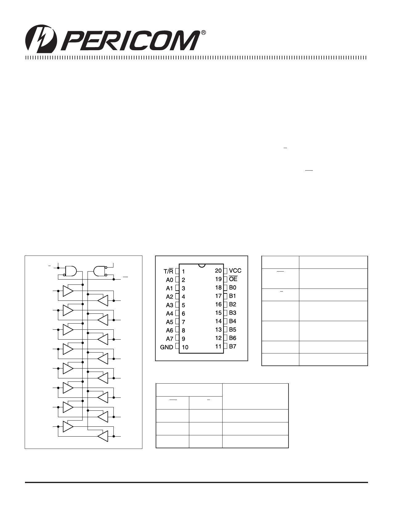
Logic Block Diagram
Product Pin Configuration Product Pin Description
T/R
OE
Pin Name Description
OE
3-State Output Enable
Inputs (Active LOW)
A0
20-PIN
T/R Direction Control Input
B0
H20
L20
A0-A7 Side A Inputs or
A1
Q20
3-State Outputs
B1
S20
A2
B2
B0-B7 Side B Inputs or
3-State Outputs
A3
GND Ground
B3
A4
B4
Truth Table(1)
VCC
Power
1A5
Inputs(1)
B5
OE
T/R
Outputs(1)
A6
B6
L
L
Bus B Data to Bus A
A7
L
H
Bus A Data to Bus B
B7
H
X
High State Z
Note:
1. H = High Voltage Level, X = Don’t Care,
L = Low Voltage Level, Z = High Impedance
1
PS2099A 02/13/97
Share Link: