STB200NF03T4(2002) Ver la hoja de datos (PDF) - STMicroelectronics
Número de pieza
componentes Descripción
Lista de partido
STB200NF03T4
(Rev.:2002)
(Rev.:2002)
STMicroelectronics

STB200NF03T4 Datasheet PDF : 14 Pages
| |||
STB200NF03/-1 STP200NF03
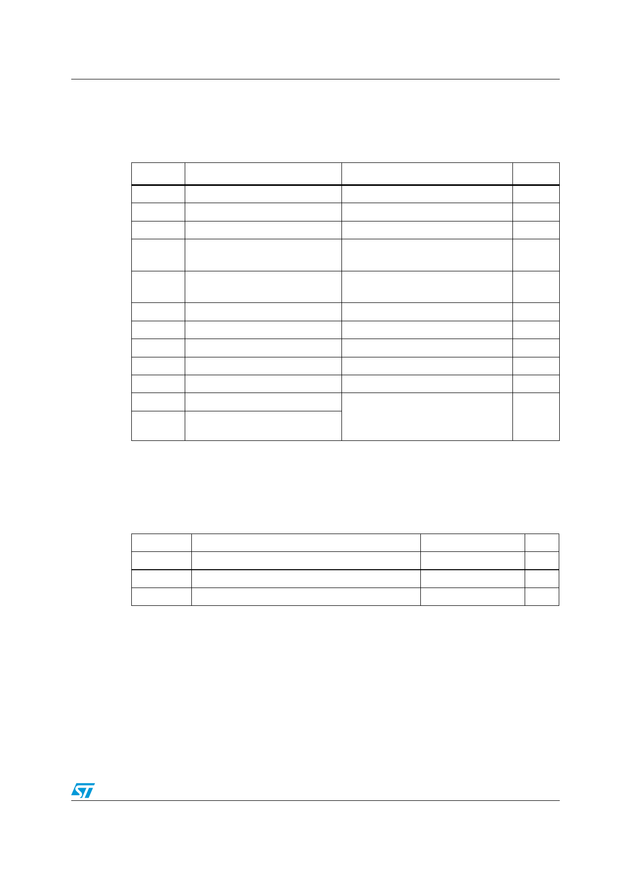
ELECTRICAL CHARACTERISTICS (continued)
SWITCHING ON
Symbol
Parameter
Test Conditions
Min. Typ. Max. Unit
td(on)
Turn-on Delay Time
VDD = 15 V
ID = 60 A
30
ns
tr
Rise Time
RG = 4.7 Ω
VGS = 10 V
195
ns
(Resistive Load, Figure 3)
Qg
Total Gate Charge
Qgs
Gate-Source Charge
Qgd
Gate-Drain Charge
VDD= 24V ID= 120A VGS= 10V
113
140
nC
32
nC
41
nC
SWITCHING OFF
Symbol
Parameter
td(off)
tf
Turn-off Delay Time
Fall Time
Test Conditions
VDD = 15 V
ID = 60 A
RG = 4.7Ω,
VGS = 10 V
(Resistive Load, Figure 3)
Min.
Typ.
75
60
Max.
Unit
ns
ns
SOURCE DRAIN DIODE
Symbol
Parameter
Test Conditions
ISD
ISDM (•)
Source-drain Current
Source-drain Current (pulsed)
VSD (*) Forward On Voltage
ISD = 120 A
VGS = 0
trr
Qrr
IRRM
Reverse Recovery Time
Reverse Recovery Charge
Reverse Recovery Current
(*)Pulsed: Pulse duration = 300 µs, duty cycle 1.5 %.
(•)Pulse width limited by safe operating area.
ISD = 120 A di/dt = 100A/µs
VDD = 25 V
Tj = 150°C
(see test circuit, Figure 5)
Min.
Typ.
70
170
5
Max.
120
480
1.3
Unit
A
A
V
ns
nC
A
Safe Operating Area
Thermal Impedance
3/14
Share Link: